 kelvinA
[12:05]
So, before I started creating a devboard that included the TC358870XBG, I wanted to see if I could find whatever QFN chip is used for the ET01-4K-V3.0 -- a named HDMI driver board on Alibaba:
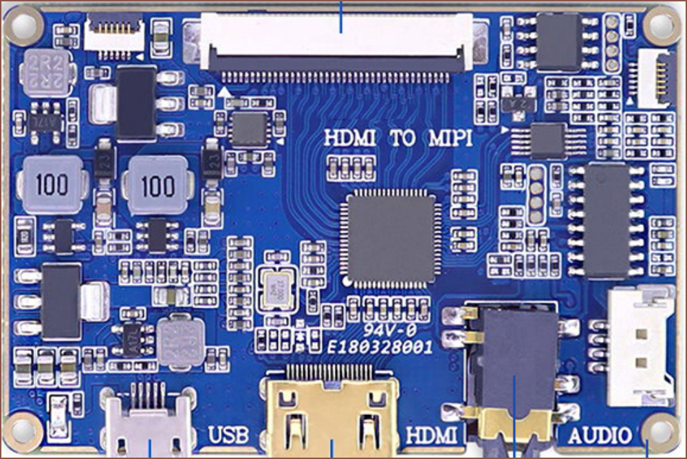
This is because It's probably easier to route out than the TC, which is a BGA package. Searching HDMI to MIPI QFN lead me to the LT6911C and LT6911UXC,.The LT6911C supports HDMI 1.4 whereas the LT6911UXC supports HDMI 2.0. On AliExpress, it seems that the former is around £6 anf the latter £9, wheras the TC358870XBG is £4.
The freely downloadable brief was extremely brief, so I messaged as many AliExpress sellers of the LT6911C as I could find and I received some documentation that at least mentioned the pinout of the chip. Unfortunately, out of all 64 pins that the chip has, I couldn't see any mention of one that changed the I2C address. I did see that it's got an I2C for "EDID" and "Program Register", however.
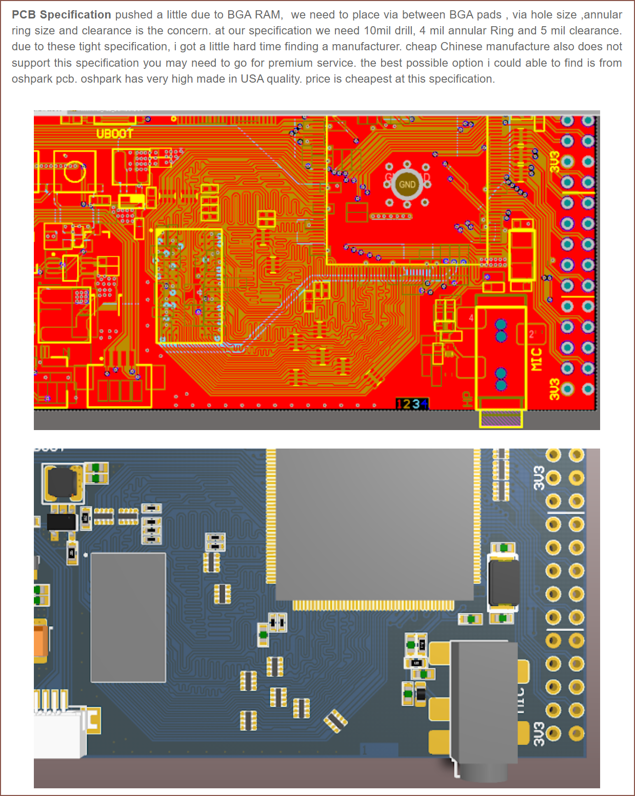
Looking at the above PCB, it's possible that this chip doesn't need an external microcontroller to initialise it, but since I don't have a fully featured tech document anyway, I'll move forward with the TC358870XBG, hoping that I don't need vias like what was needed for a DDR3 chip on a board I found on my research travels:
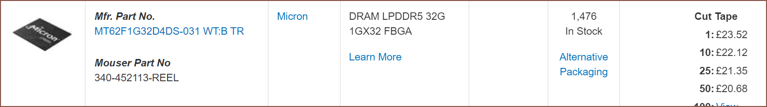
At least I found out that a 32GB chip of LPDDR5 is £23/each as a result of this research:
[17:40] JLC has the TC358870XBG and, as such, the footprint is available on EasyEDA. Very quickly looking over the pinout, it seems that the traces for the interior would look something like this:
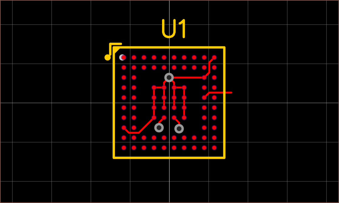
These are 0.12mm traces with 0.12mm spacing set in the DRC. JLC claims that, for 4+ layer boards, their capabilities are down to 0.09mm track/space. They also say their minimum BGA pad size is 0.25mm, and they're 0.24mm in this EasyEDA footprint. The bottom 2 pads in the middle group of balls are for TEST and IR, and I doubt I'd be using it so it should "be fixed low", according to the documentation. I'm assuming they're saying to just connect it to ground. The TEST pin also has the note to always fix low externally too, so it's probably safe to assume that entire interior section can just be one GND copper pour.
In any case, all this talk about HDMI to MIPI bridges are irrelevant if the Tetrinsic proof-of-concept ergonomically fails.
Discussions
Become a Hackaday.io Member
Create an account to leave a comment. Already have an account? Log In.