 Scott Gillins
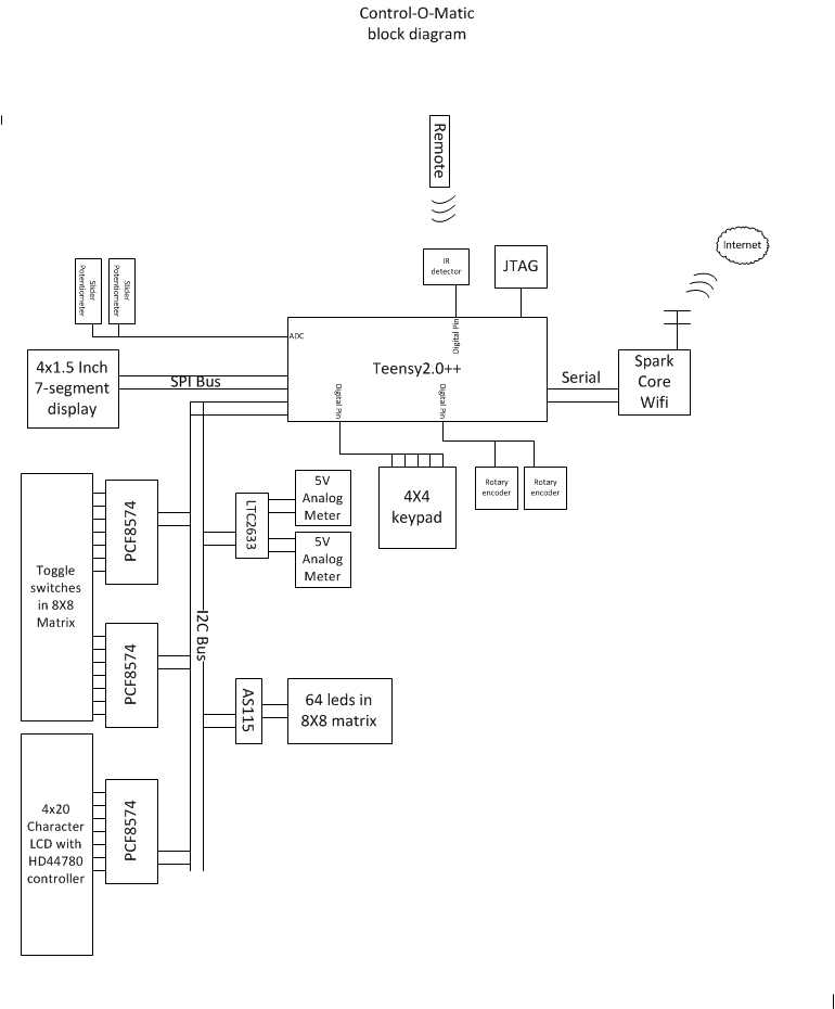
As I started to put together the documentation for this project of mine I realized that a traditional schematic would not provide much value since I used several dev boards and did not have one big PCB that had all the parts on it. Since you still need to understand how it is all put together I have crafted a little block diagram to show how the major pieces are connected. I plan to put together some more details on the individual blocks as time allows. Maybe in version 2.0 I will integrate all the pieces into a single PCB. I know it would make assembly a lot easier than it was this time.
Discussions
Become a Hackaday.io Member
Create an account to leave a comment. Already have an account? Log In.