 zpekic
The hardware for this project is a combination of FPGA and discrete ICs wired on the breadboard:
- Digilent Anvyl board is used - I like it because it has ample connections (7 8-bit PMODs plus 10-bit dedicated pins for breadboard). However, it is no longer available on Digilent store, but can be replaced with any board that has sufficient digital I/O pins.
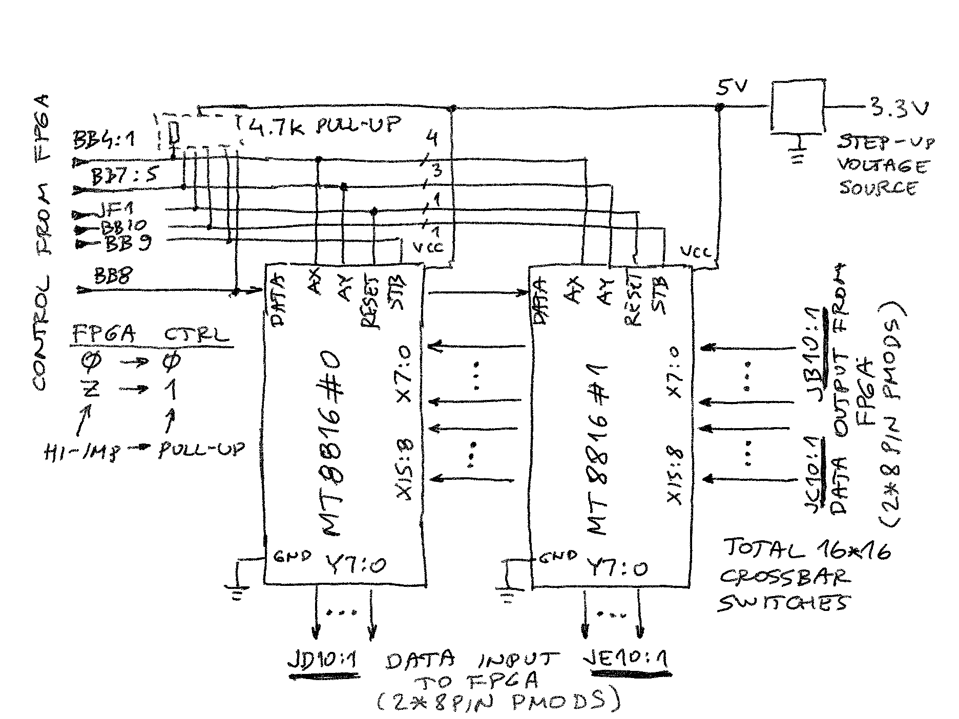
- 2 MT8816 chips, Digilent 3.3V to 5V "PowerBrick", bunch of wires and few 4.7k SIP resistor packs (pull-ups to 5V)
The 2 MT8816 chips implement the cross-bar switch matrix (2 * 8 * 16 = 16 rows * 16 columns), while the rest of the system is implemented inside the FPGA:
Few things to note:
MT8816 are "analog switches" - meaning that voltage on inputs is reflected on outputs. This works well with FPGA board because it operates with 3.3V digital I/O pins, so that same voltage level can be picked up as input. Therefore no special voltage level adaptation is needed on X and Y cross-bar connections (also they are interchangeable, in this design X is output, Y is input (looking from the FPGA)
To implement "wire OR" on inputs, FPGA I/O pins are programmed with pull-down, for example PMOD "JD" that receives Y7:0:
## JD
    NET "JD1"    LOC = AB13    |    PULLDOWN    |    IOSTANDARD=LVCMOS33;    #Bank = 2, pin name = IO_L41N_VREF_2,            Sch name = JD1
    NET "JD2"    LOC = Y12    |    PULLDOWN    |    IOSTANDARD=LVCMOS33;    #Bank = 2, pin name = IO_L42N_2,                        Sch name = JD2
    NET "JD3"    LOC = T11    |    PULLDOWN    |    IOSTANDARD=LVCMOS33;    #Bank = 2, pin name = IO_L43N_2,                        Sch name = JD3
    NET "JD4"    LOC = W10    |    PULLDOWN    |    IOSTANDARD=LVCMOS33;    #Bank = 2, pin name = IO_L44N_2,                        Sch name = JD4
    NET "JD7"    LOC = W12    |    PULLDOWN    |    IOSTANDARD=LVCMOS33;    #Bank = 2, pin name = IO_L42P_2,                        Sch name = JD7
    NET "JD8"    LOC = R11    |    PULLDOWN    |    IOSTANDARD=LVCMOS33;    #Bank = 2, pin name = IO_L43P_2,                        Sch name = JD8
    NET "JD9"    LOC = V11    |    PULLDOWN    |    IOSTANDARD=LVCMOS33;    #Bank = 2, pin name = IO_L44P_2,                        Sch name = JD9
    NET "JD10"    LOC= T10        |    PULLDOWN    |    IOSTANDARD=LVCMOS33;    #Bank = 2, pin name = IO_L45P_2,
The M8816 must be powered with usual 5V / GND - that's where the PowerBRICK comes into play as simple and convenient way to boost 3.3V to 5V
The control signals to MT8816 must be TTL compatible. There are of course ICs that can do safe and efficient signal level conversion, but for the breadboard has no place for those. Instead, a trick was used:
- All control signals (RESET, AX, AY, DATA, STROBE) are pulled up to 5V via resistors
- If "1" level is desired on these outputs, the FPGA pin is put to "Z" tri-state, floating it up to valid "1" level above V1L
- If "0" level is desired on these outputs, a "0" is output by the FPGA to pull down the resistors below the V0H
-- control bus ('Z' with external 4k7 resistor and pull-up mode give 0.26V low and 5.0V hi)
MT_AX0 <= 'Z' when (mt_ctrl(0) = '1') else '0';
MT_AX1 <= 'Z' when (mt_ctrl(1) = '1') else '0';
MT_AX2 <= 'Z' when (mt_ctrl(2) = '1') else '0';
MT_AX3 <= 'Z' when (mt_ctrl(3) = '1') else '0';
MT_AY0 <= 'Z' when (mt_ctrl(4) = '1') else '0';
MT_AY1 <= 'Z' when (mt_ctrl(5) = '1') else '0';
MT_AY2 <= 'Z' when (mt_ctrl(6) = '1') else '0';
MT_DATA <= 'Z' when (mt_ctrl(8) = '1') else '0';
MT_STROBE0 <= 'Z' when ((phi1 and (mt_ctrl(8) or mt_ctrl(9)) and (not mt_ctrl(7))) = '1') else '0';
MT_STROBE1 <= 'Z' when ((phi1 and (mt_ctrl(8) or mt_ctrl(9)) and mt_ctrl(7)) = '1') else '0';
MT_RESET <= 'Z' when ((mt_ctrl(8) and mt_ctrl(9)) = '1') else '0';
This works well except the speed - a RC circuit is introduced which needs time to charge/discharge, and a result the whole system does not work reliable above 1.5MHz clock speed. But that is of no importance for this proof of concept.
From the FPGA perspective, this outside cross-bar switch appears as a 16*16 matrix of 1-bit write-only memory (state of switch can be set, but not read back). Following operations are supported:
- no change (both STROBE signals held low during microcode cycle)
- turn on a switch (DATA is high, STROBE selecting appropriate MT8816 high, switch selected through AX and AY)
- turn off switch (as above, except DATA is low)
- turn off all switches ("nuke" in microcode, both RESET signals are tied together and pulsed high)
The above requires 6 signals in 3 fields defined in the microcode:
// System interface signals
MT_CTRL        .valfield 2 values
            nop,
            on,
            off,
            clear default nop;

MT_ROW        .valfield 4 values * default 0;
MT_COL        .valfield 4 values * default 0;
In order to observe the right MT8816 control signal timing (set up and hold times), a 4-phase clock is introduced and some signals are enabled only during the right phase:
-- 4 phase clock to activate strobe at right time
phi0 <= '1' when (mt_cnt = "00") else '0';
phi1 <= '1' when (mt_cnt = "01") else '0';
phi2 <= '1' when (mt_cnt = "10") else '0';
phi3 <= '1' when (mt_cnt = "11") else '0';
Discussions
Become a Hackaday.io Member
Create an account to leave a comment. Already have an account? Log In.