 Dave Collins
Update: PCBWay has kindly offered to sponsor the cost of the next run of boards! This is amazing, as I was planning on doing a comparison between JLC and PCBWay in my next post. Follow this space for more soon!
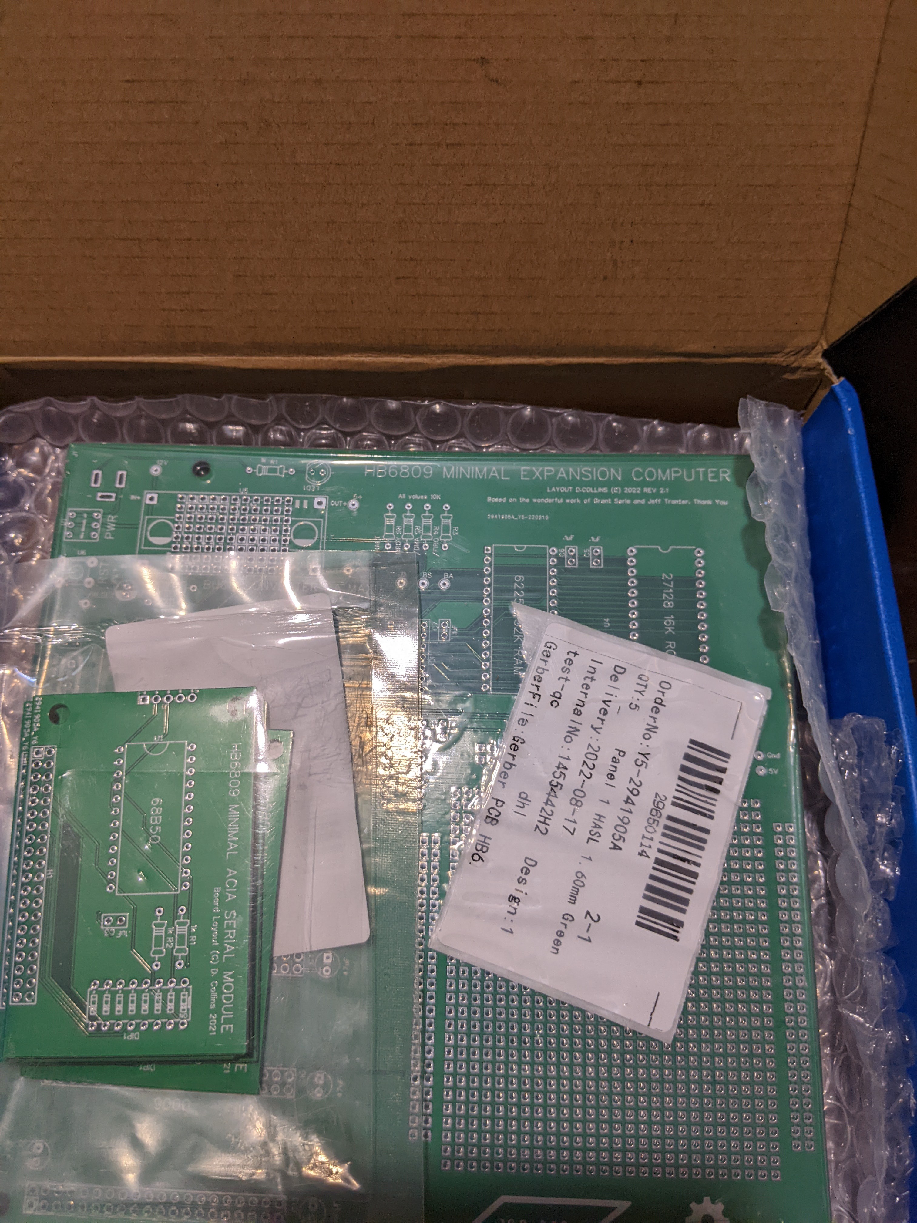
The boards:
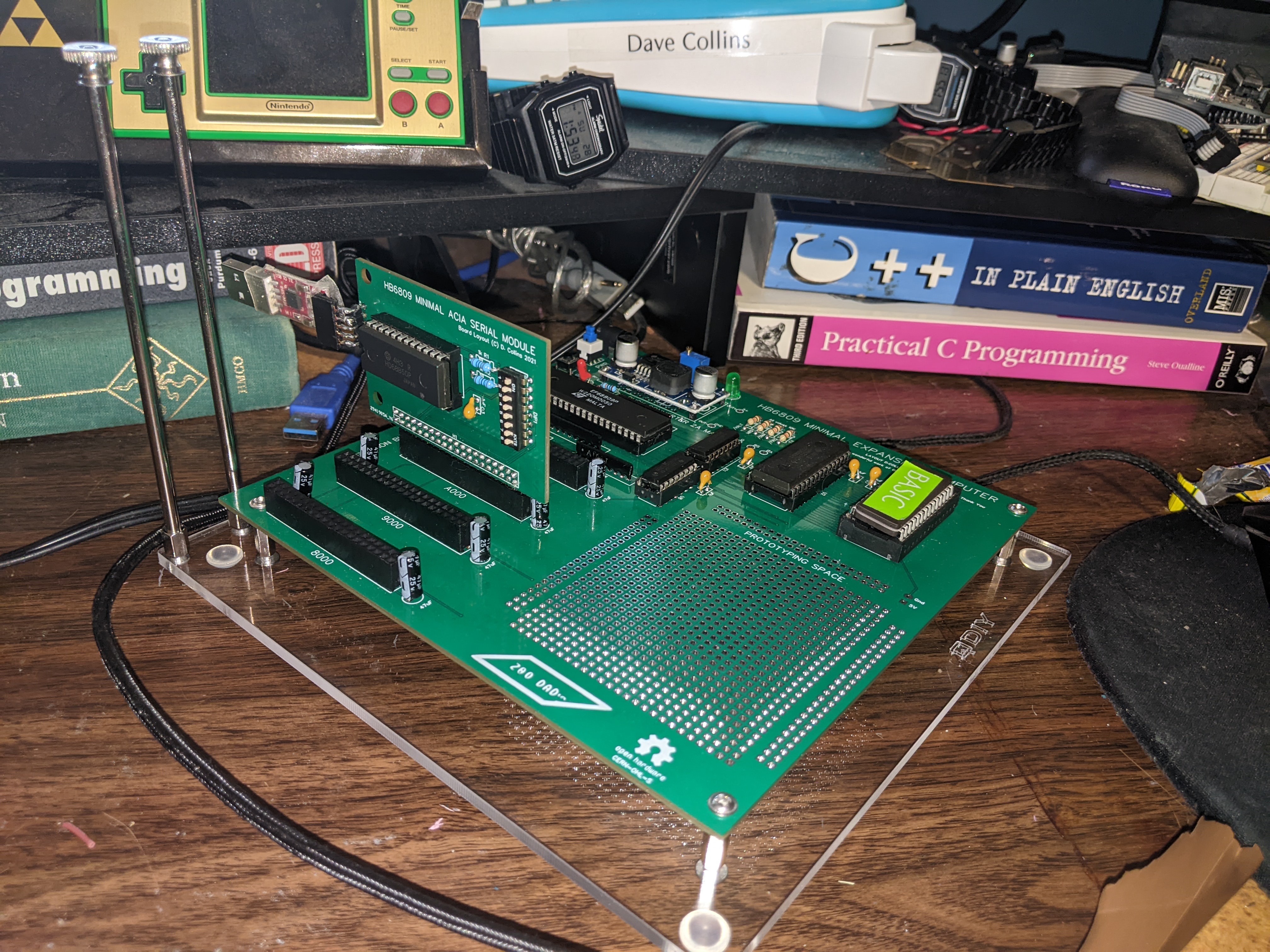
The Boards Were received when the manufacturer stated they would be here. Both the AICA board and the main PCB were packaged with care, there was minor shipping damage to the box but the goods came unhindered inside the packaging. This shipping damage was just slight box crumpling, that could be more blamed on the shipper DHL, than anyone but to be honest I've received things from amazon in far worse shape.
Fixing the Issues:
After buildup, the main PCB had some issues. The first big problem I ran into was the addressing on the schematics (which in turn translated to the layout) for the EPROM:
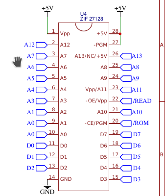
As you can see the A0-2 have potential issues. When i probed the R//W line coming from the CPU with the scope looking for issues I determined that it was basically at it's high state, essentially just reading and probing through the address lines. Upon checking the decode logic I found this to be the case as the selector would simply run through the selected lines over and over again. Fortunately, this wasn't hard to fix, I simply cut the two traces (one between pins 10 and 9, and the trace going A1 on the ram running from pin 8.) Then after that was done I bodged the two pins with silicone jacketed flexible patch wire.
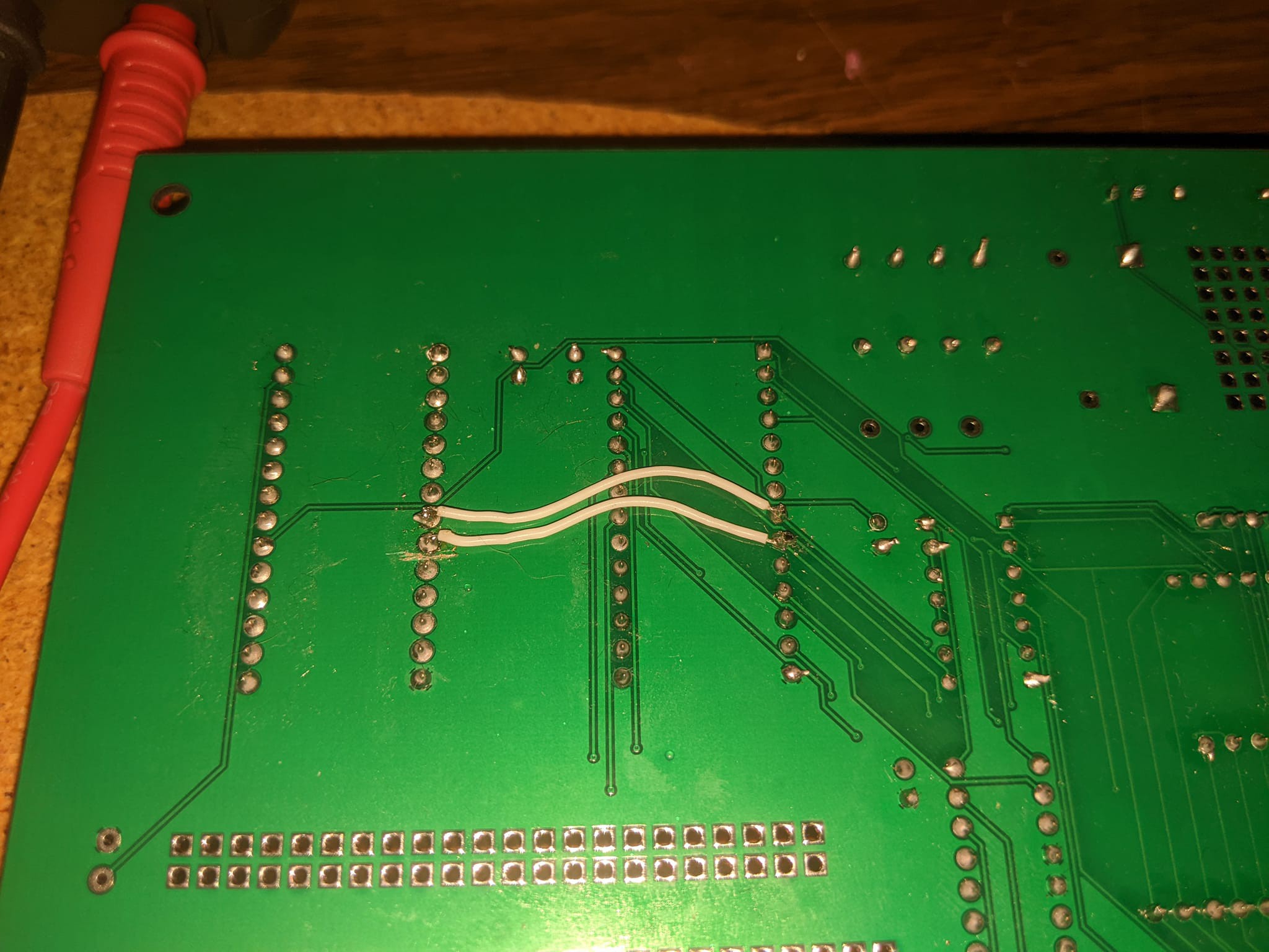
After doing this I got much more normal r//w readings with every so often it switching between the two signals as it processed through the loop for the machine language monitor. The other issues were a handful of silly auto-router related mistakes such as a few lines running through a plated through hole section and the +5V and GND nets being routed throughout the project because when I went to finish up the remaining routing with the auto router I forgot to select them to skip the routing.
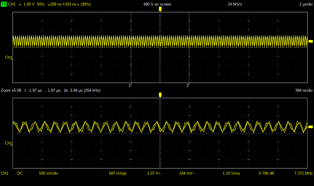
I have a very minimal scope, so unfortunately these screenshots are not super great but they basically demonstrate everything is fine with the board:
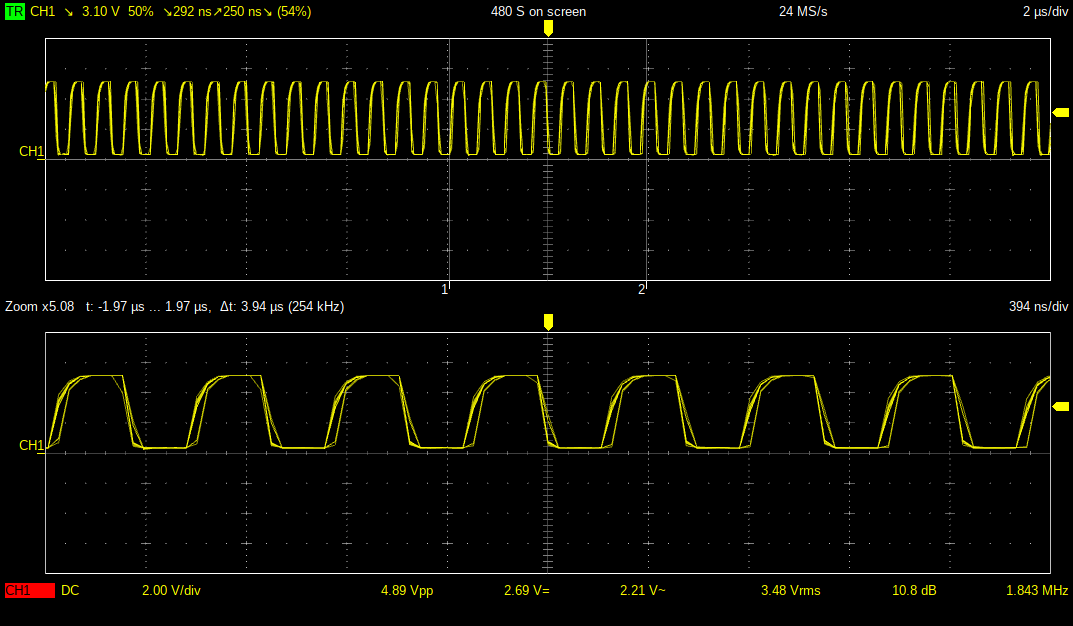
CLK (Tests the crystal oscillator)
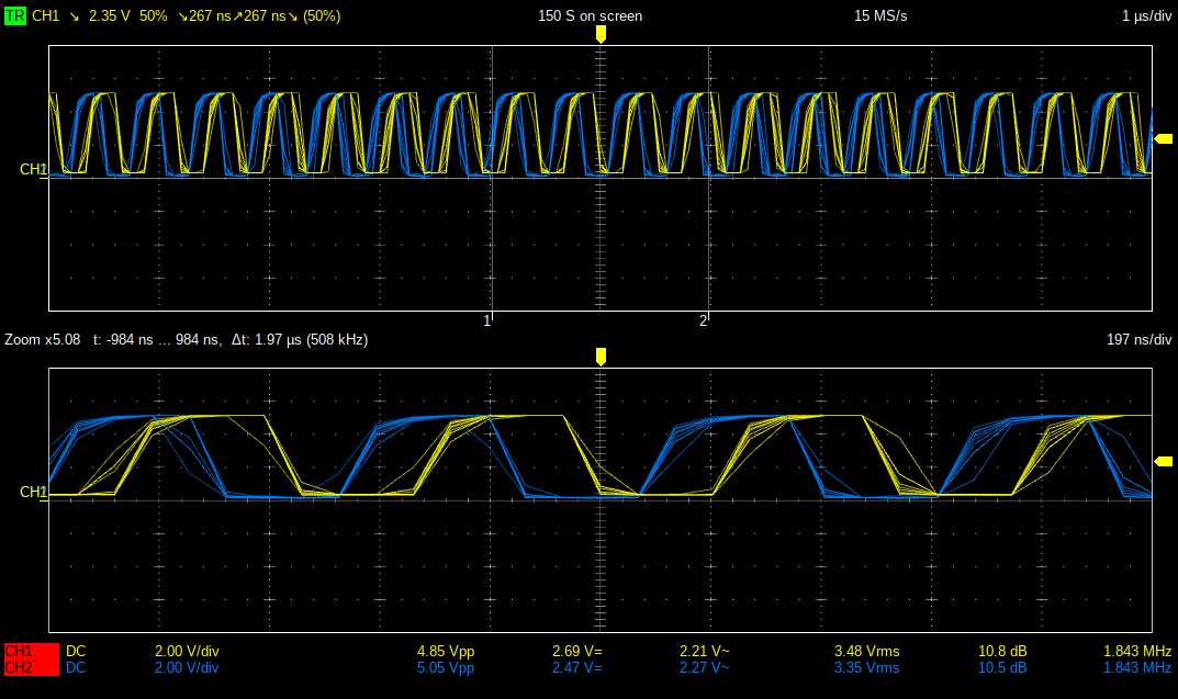
E (Tests the internal clock frequency):
E&Q (Tests the internal clock divider / clock generator ):
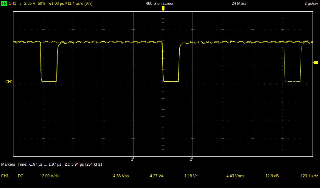
R/W:
Determine's if the CPU is running through code, This would be constantly high if there was an issue, or the cpu was not sitting at the ASSIST9 ready prompt.
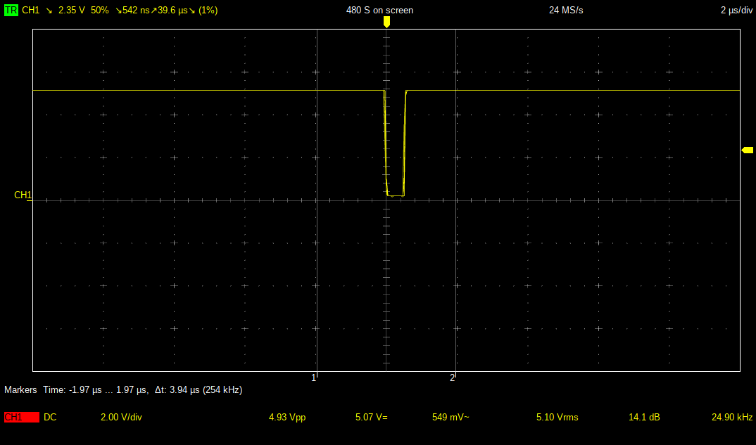
A000 (Shows the ACIA is being selected every so often for read checks):
I spent some time fixing the routing issues with the PCB and adding a probe point for the R//W lines moving some of the packages closer to where they are used and moving the points so they don't introduce unnecessary issues (especially with routeing). I also brought the individual pull up resistors for the unused signal lines closer to the rest of the termination. This allowed the RAM and ROM to be routed much easier.
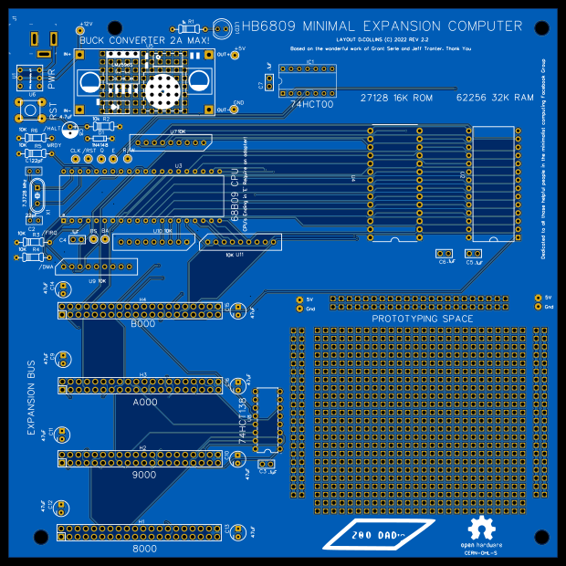
As you can see I shrunk the prototype space to include more empty space to route into I put the RAM /ROM selection gates at the top and I moved all of the chip labels off the actual socket footprint to make this easier to read once the chips are installed in the sockets. The +5V Fill is on the top, with the GND Fill on the bottom. I Joined the "island" planes in spaces using vias with .6 mm traces (these are double width the same size as the +12V Tracks leading to the switch and the DC-DC converter). Since the 5v and GND were not double routed, there were places that it needed to be linked up.
I Tested the Fit on the PCB mounting holes, which was perfect! Here it is mounted to an open frame Mini-ITX platform. The mounting rails for the single PCI-E slot in this form factor lines up perfectly with the right angle connector for the card edge being mounted coming out of the back side of the PCB. So when I get around to making a display adapter the card should fit into the rails with a 3d Printed mounting bracket, the ports on the edge of the card should fall well in between the rails.
What's next:
I am getting ready to send off the revisions to have a final run of the main PCB. The Serial card works perfectly, and won't actually need any further work. This time i'll be using a different PCB manufacturer PCBWay, so that I can compare the build quality. I have always been really impressed with the Asian market rapid turn PCB manufacturers, so I am not overly concerned but I like writing about these things as much as I like working on them, so it should be a good experience!
After I verify the PCB's are working, I'll consider this stage of the project more or less completed. Once I know they wok for me I'll release the Gerber files for anybody to try out, and most likely sell any extra boards to anybody who wants them for the cost of shipping (I don't need 10 blank boards just hanging around). I have several plans for expansion modules - a video adapter, a sound card, and a Zilog SIO serial board with a RS-232 port (as well as TTL hook ups!).
Thank you for taking the time to read about this project thus far. I really do hope to soon be able to share the project files, including the easyEDA files, so that if somebody wants to further play around with this design they may.
Discussions
Become a Hackaday.io Member
Create an account to leave a comment. Already have an account? Log In.