 agp.cooper
Schematic and PCB
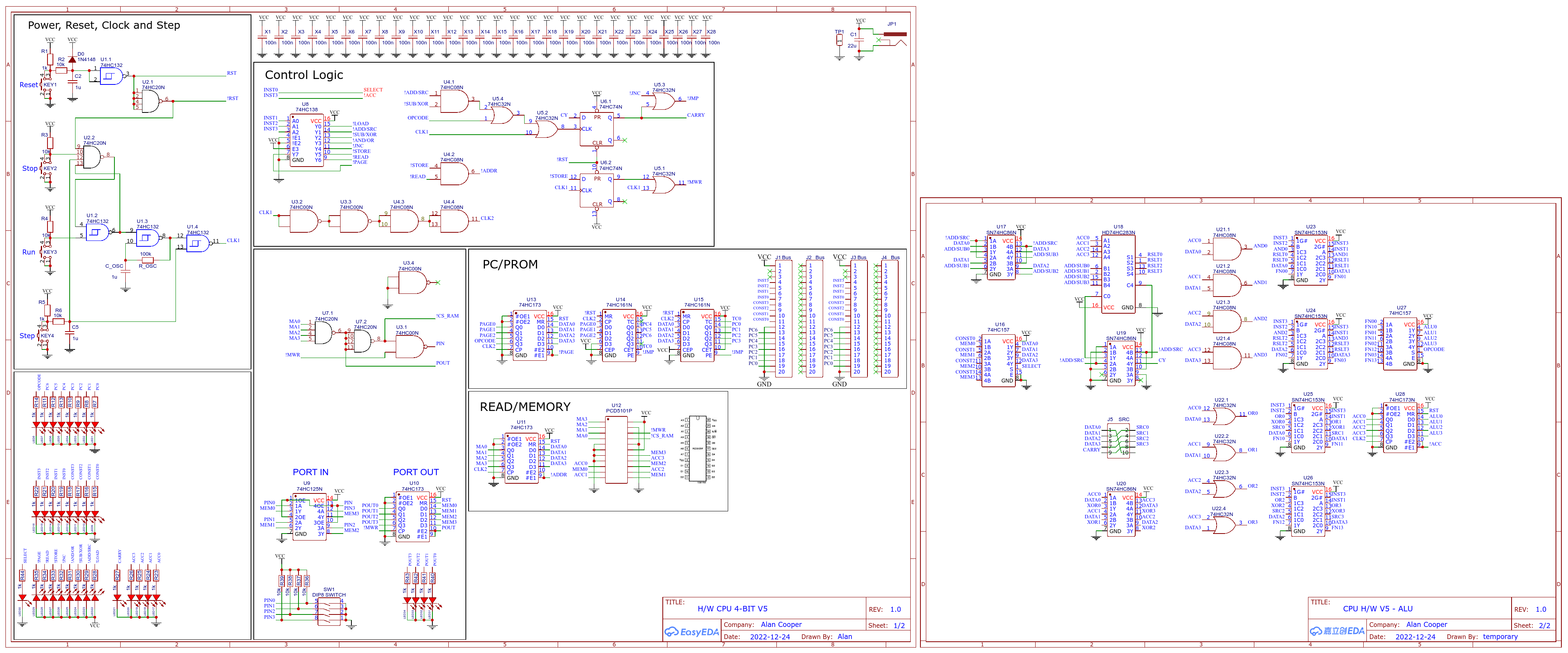
Started the schematic design, the ALU is pretty well all new, so it will take time.
The layout will be important as the auto-router will struggle with this many chips.
---
The 16 byte diode PROM boards arrived today. Two boards will have nearly 400 components, so they will take a while to solder.
---
Some updates to the simulation model.
---
Some progress on the schematic, trying to group the chips:
Instruction Set Again
The minimum instruction set is:
- LOAD
- ADD
- NAND
- ?
- JNC
- STORE
- READ
- PAGE
Missing are instructions like LEA, CALL and RTN, etc, but these require structural changes.
Subtraction is pretty easy to do, I will use reference variables here.
A = A SUB B:
- READ A
- LOAD M
- NAND F
- READ B
- ADD M
- NAND F
- STORE C
Test if equal:
- READ A
- LOAD M
- NAND F
- READ B
- ADD B
- NAND F
- ADD F
- JNC [A != B]
- ... [A == B]
Test if bits are HIGH:
- READ A
- LOAD M
- NAND F
- NAND MASK
- ADD 1
- JNC [false]
- ... [true]
Test if bits are LOW:
- READ A
- LOAD M
- NAND MASK
- ADD 1
- JNC [false]
- ... [true]
Other logic gates can be derived from the NAND gate, but may require memory to store intermediate results. Although NAND can replace XOR in many cases, XOR is "necessary" for efficient toggling of bits.
An alternate instruction set is:
- LOAD
- ADD
- AND
- XOR
- JNC
- STORE
- READ
- PAGE
Subtraction is using XOR.
A = A SUB B:
- READ A
- LOAD M
- XOR F
- READ B
- ADD B
- XOR F
- STORE C
Test if equal:
- READ A
- LOAD M
- XOR F
- READ B
- ADD M
- XOR F
- ADD F
- JNC [A != B]
- ... [A == B]
Test if bits are HIGH:
- READ A
- LOAD M
- AND MASK
- ADD F
- JNC [false]
- ... [true]
Test if bits are LOW:
- READ A
- LOAD M
- XOR F
- AND MASK
- ADD F
- JNC [false]
- ... [true]
OR is awkward, using memory reference here again:
- READ A ; Set memory reference A
- LOAD M ; Using memory reference
- XOR F
- STORE C ; Save intermediate result
- READ B ; Set memory reference B
- LOAD M ; Using memory reference
- XOR F
- READ C ; Set memory reference C
- AND M ; Uses address from previous store
- XOR F
- STORE C ; Save result to C
Compared to AND:
- READ A ; Set memory reference
- LOAD M ; Using memory reference
- READ B ; Set memory reference
- AND M ; Uses address from previous store
- STORE C ; Save result to C
Compared to XOR using NANDs:
- READ A ; Operand A
- LOAD M
- READ B ; Operand B
- NAND M
- STORE C ; Intermediate result
- READ B
- NAND M
- STORE D ; Intermediate result
- READ C
- LOAD M
- READ A
- NAND M
- READ D
- NAND M
- STORE C ; Save result in C
AND versus NAND
While AND has the advantage that the logic in the general use case is slightly simpler.
If I need to free up an op code slot (i.e. the XOR slot), the NAND op code is the way to go.
Second Thoughts
Not a lot to gain from the second op code page. I think I should have spent my time looking at structural changes.
There are efficient algorithms for multiplication and division that only use ADD and NAND, so SAR and SAL and not required op codes.
Where to Next?
May be a stack to push/pop return addresses and intermediate results?
Eventually I want to look at a single cycle Von Neumann architecture.
AlanX
Discussions
Become a Hackaday.io Member
Create an account to leave a comment. Already have an account? Log In.
Yes absolutely, it was a missed opportunity, and I did want to try it.
I do have a box of DIP switches and diodes, but really I am not looking forward to soldering 400 components.
Regards AlanX
Are you sure? yes | no
Surely the PROM board is a prime candidate for PCB assembly to save your eyesight and yourself from RSI?
Or do you have a whole box of diodes and DIP switches you want to "use up"?
Are you sure? yes | no