 Eric Hertz
If you haven't been following the drama, feel free to scroll down to the pictures.
Looking back at previous logs... And making some notes regarding measurements at the motherboard (in that previous log)...
It looks like the only signal that *might* need to be pulled to some value is /LOCK. I've since pulled this up (by accident) via 10K resistor with no noticeable effect. Then I noticed that the point was to lock other devices *out* of using the bus, so instead pulled it low. This time with a 100-ohm resistor (which should be plenty for an LS-TTL input).
I didn't 'scope when /LOCK was pulled high... but earlier with /LOCK pulled low I wasn't getting an ALE signal, but I *did* have /AEN = LOW and CEN = HIGH, that time.
So why no ALE...? Weird.
As I understand: /LOCK shouldn't affect the 8288, its purpose is to tell other devices not to use the bus, because the 8088's performing a read-modify-write, which without /LOCK could be modified by another device *during* the RMW. Thus, /LOCK shouldn't be fed-back to the 8288, because the 8088 *has to* perform a W after the R (unless the 8288 *only* allows write thereafter? What? No... it can't be... the only control-inputs are AEN and CEN, and those are both correct.)
(And... does /LOCK actually prevent the DMA_HRQ->HOLDA?!)
---------
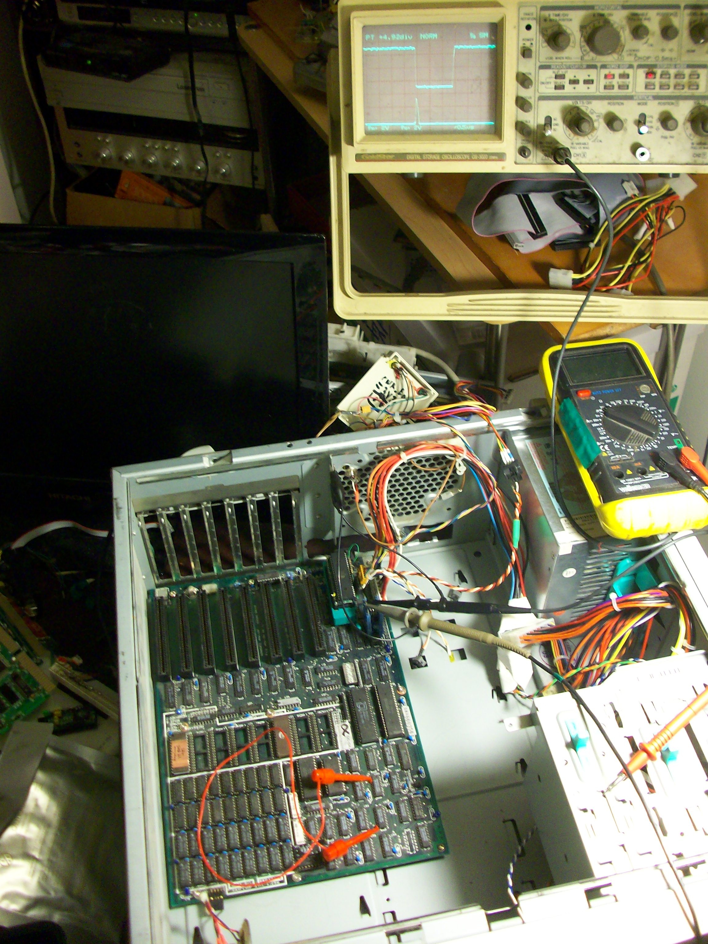
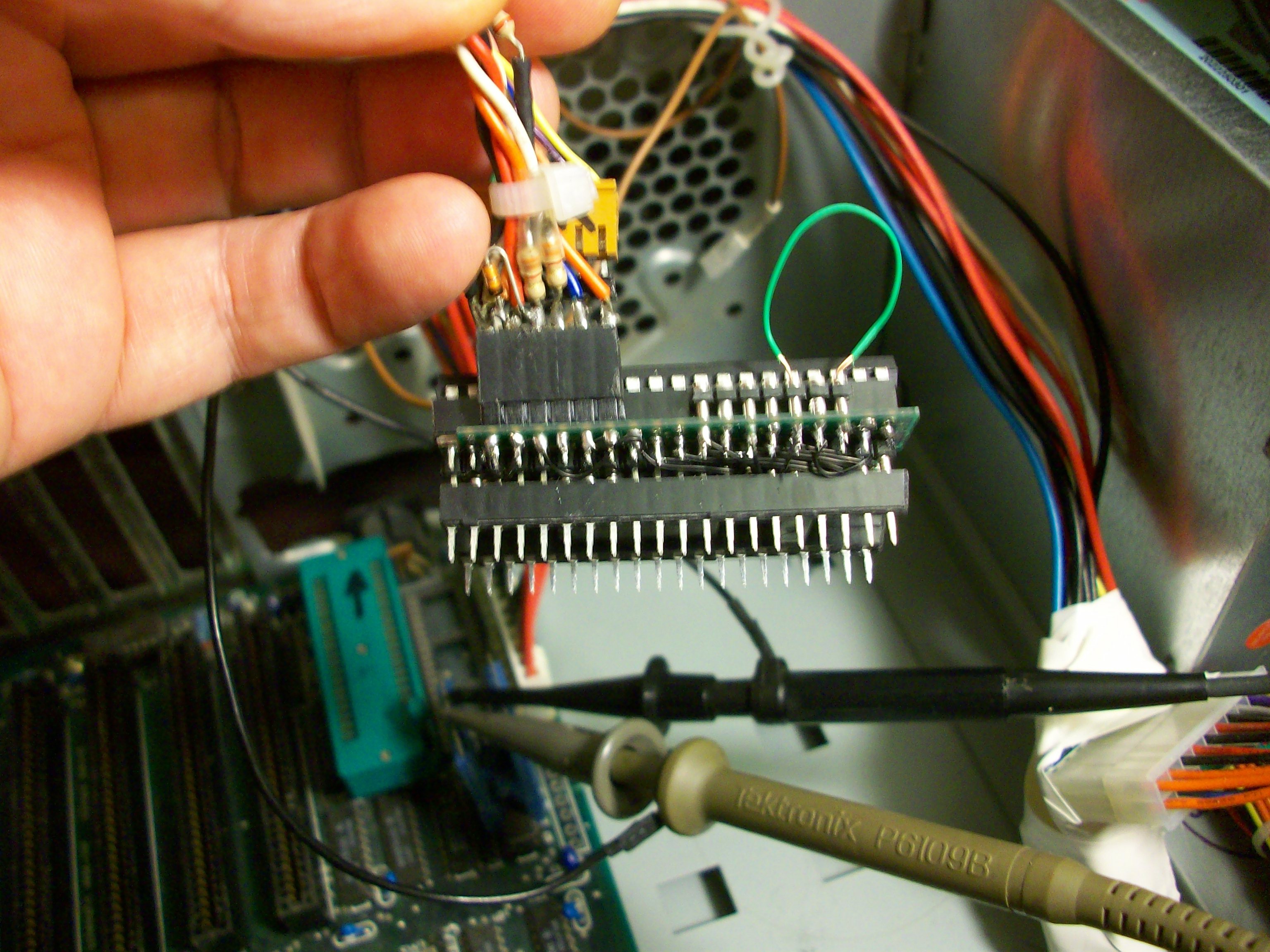
Turns out, my "chip-clip" attached to the 8288 is a bit flakey, and at one point I measured shorts between a couple pins. Combine that with the fact the 8288's pins don't actually exit the chip in the same way most do horizontal-then-bent-downward... This guy bends straight downward, leaving nothing for the chip-clip to align on, and requiring its pins to be bent beyond the aligning-plastic.
Moved it around, more carefully, and... Oh, I also located the /LOCK signal's destination (one input of a 4-input NAND, matching the schematic), and tied that directly to ground, (I cut out the resistor pull-down, 'cause it was too hard to work with, located on my breakout-board under the AVR).
...and...
We Have Data.
The ROM on the far-left is the BIOS (actually a copy, because I didn't want to risk damage to the original). The second ROM chip is actually the "Extension ROM" I made earlier.
AVR in a breakout-board mounted in a ZIF socket with combined ISP header and UART output dangling to the right. 'Scope shows /S1 which is driven low during a read-memory request by the AVR (or 8088) (top trace). The bottom trace shows the ALE output from the 8288. Note that ALE is <=1 bus-clock, so you can clearly see that the bus-transaction is taking *way* more than the allotted 4 cycles. (Artificial wait-states inserted by the AVR, and working!)
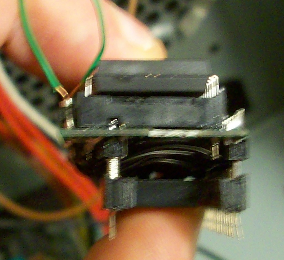
It's hard to see the clock-inverter/delay jumper, but it's the green wire behind the ISP header. Currently it's set to the output of the first inverter (I determined it should probably be connected to the output of the fifth, but I moved it around in earlier tests and forgot to move it back. Regardless, it's working! So, maybe all that worrying about meeting specific timings was a bit over-done... Par for the course.Also interestingly, the READY processing code works! I was afraid it wouldn't, because it takes several AVR instructions to read a pin, compare it, then jump, and all of that is supposed to happen in a single clock-cycle. But it works!
Looks like we're *right at* the limit of this analog/digital 'scope's digital abilities... It looks like I'm getting about 4-5 samples during each clock-cycle... which would make sense, it's a "20MHz" 'scope, in analog-mode... Don't recall seeing specs for the number of samples/sec in digital mode, but it's old (1980's), and 20MS/s sounds reasonable. (One nice thing about this 'scope is the fact it can switch between the two modes... I've actually managed to troubleshoot serial data-streams upwards of 100Mb/s in analog-mode).
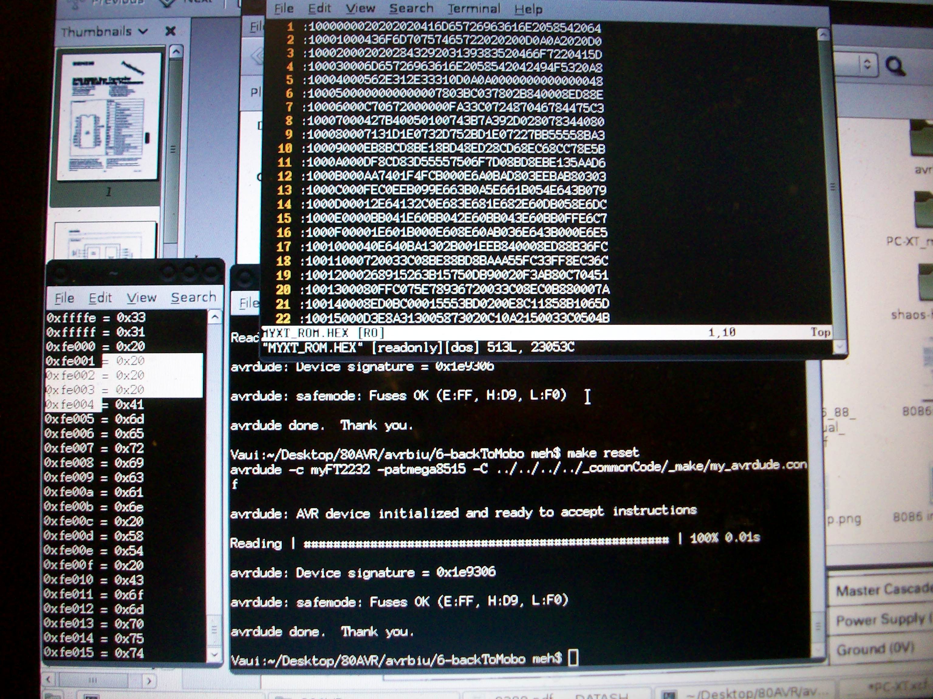
Here we have the serial-output on the left, showing the address and the read-back value. And that compares to the intel-hex dump of my ROM, which I did a while-back in my [E]EPROM programmer.
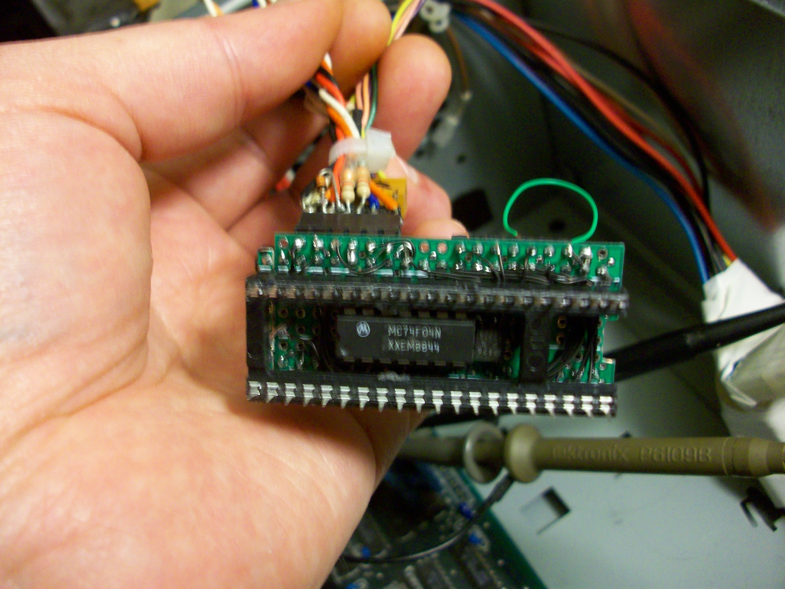
The 74F04 inverts the clock-signal, because the AVR works on rising-edge clocks, while the 8088's bus-interface expects the changes near (actually, slightly after) the falling-edges. The inverters are daisy-chained so I can select differing amounts of delays.
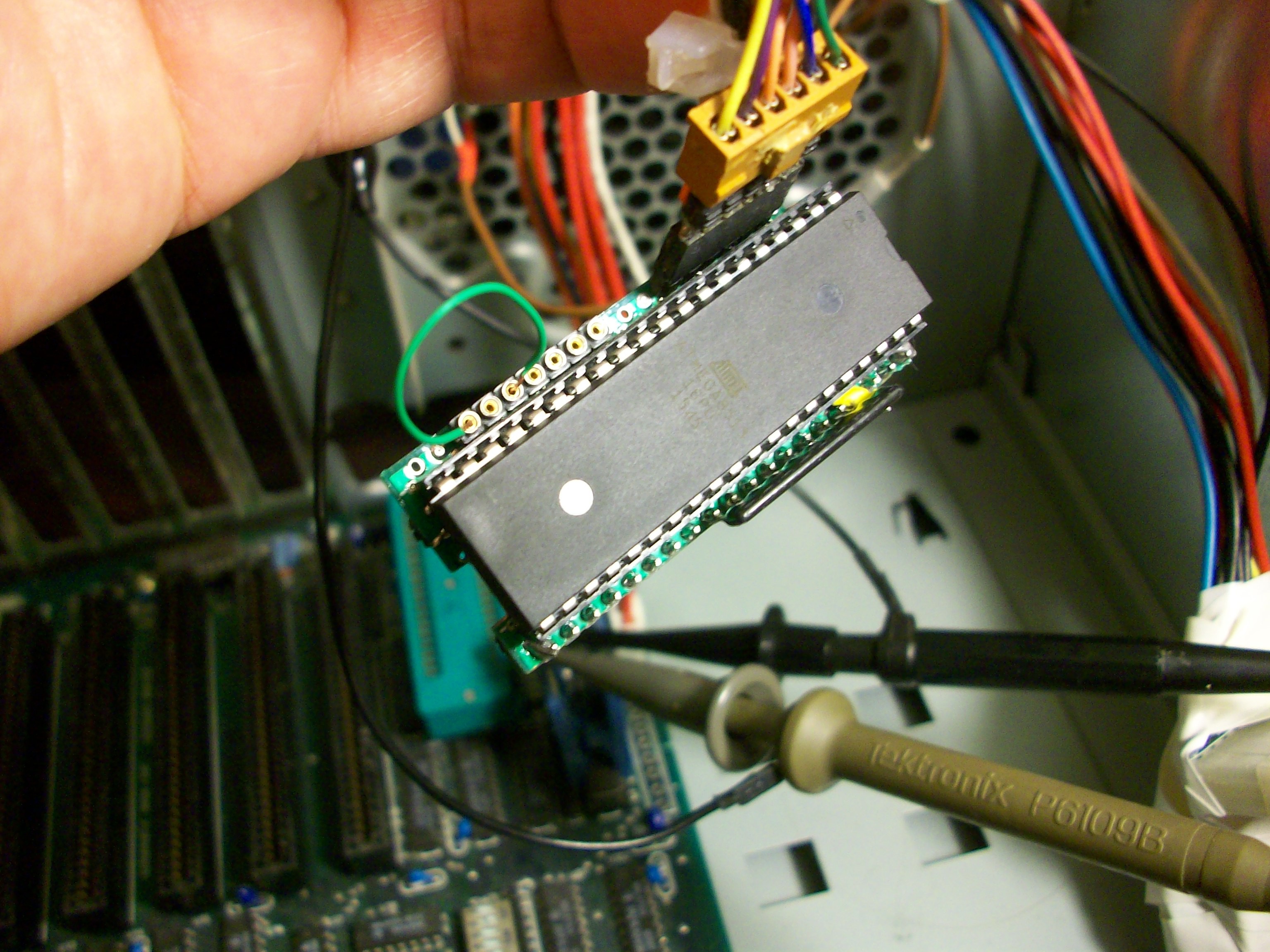
You can also see the 2N2222, used to invert the 8088's active-high RESET signal for the AVR's active-low, AND to isolate the In-System-Programmer's reset signal from the rest of the PC/XT motherboard.
The ISP header is wired-up at the top. All those resistors, wires, and diodes are part of my ISP dongle, allowing for a debug LED, a debug pushbutton, a reset button, and UART I/O all multiplexed on the ISP's header pins.
The green wire is currently jumpered to select the first inverter for the clock-signal. The network-resistor pulls up the A/D pins, which when driven by the bus (during "Read" requests) are driven by a TTL-LS, whose VOH-min is lower than the AVR's VIH-min. Apparently it's not uncommon to use pull-up resistors to interface TTL outputs to CMOS inputs... I found it in a app-note, and wrote about it in a previous log.
Here's an interesting thing:
 Shitty picture, but gets the point across... The sockets I used have a notch under them which I imagine is for exactly the purpose used, here... A row of pins can be soldered under it and protrude through the board, without interfering with the socket. Handy!
I used regular ol' header-pins for the 8088 pinout, then squished those into another socket whose pins are thinner and more like IC pins, to more-easily insert into sockets. (Squishing the header-pins into that socket required a lot of force, using a vice). I've done this once before, for this project, actually... when I made the ROM replacement for the SCSI card. Gotta make due with what I've got available!
You might've also noticed... I actually wire-wrapped to the header-pins (before crimping the socket onto it). That way the majority of the wiring could all be on the same side of the board... and gave me a reason to use my wire-wrapper, besides its handy stripper which I use all the time. So, they're wire-wrapped to the 8088's pinout, but soldered to the ATmega8515's socket. This also gave me some flexibility to run wires between header-pins.
But... there are a few pins (not currently implemented) which would be quite difficult to solder to, now that the whole thing's assembled. Ah well. I'm sure I can figure something out, should the time come.
-------------
Here's the code, extensive comments removed:
uint8_t bus88_read(uint8_t s20, uint32_t address)
{
   uint8_t data;
 //### Bus is idle (assumed) ###

   //So, it should be OK to prep our Address bytes
   ADDR1916_PORT   = (uint8_t)(address>>16);
   ADDR158_PORT    = (uint8_t)(address>>8);
   ADDRDATA70_PORT = (uint8_t)(address);

   //Begin the Bus transaction
   S20_PORT       = s20;   // OUTPUT, AROUND: ¯|_
   // The 8288 will bring ALE High...
 // ¯|_  ### T1 ###
   // The 8288 will bring ALE Low in 4-15ns after _|¯

   //Nothing to do?!
   // Gotta keep the timing aligned...
   asm("nop;");

 // ¯|_  ### T2 ###
   ADDRDATA70_DDR = ALL_INS; // >10ns AFTER ¯|_
 // ¯|_  ### T3 / Tw ###
   while(!(READY_PIN & READY_MASK))  {};  //INPUT: <30ns AFTER _|¯
   data = ADDRDATA70_PIN;

   //NOTE That we'll be in a later Tw, at this point... weeee!
   //Indicate that we're done with wait-states, and ready to enter T4
   //8088: TCLSH Status Inactive Delay: after ¯|_ 10-130ns
   S20_PORT = S20_BUS_IDLE; //OUTPUT: >10ns AFTER ¯|_
 // ¯|_  ### T4 ###
   // The 8288 will bring /IOR, /IOW, etc. high within 10-35ns of ¯|_
   //Nothing to do?!
   asm("nop;");

 // ¯|_  ### BUS IDLE ###
   // WARNING: This is NOT compatible with DMA and 8087!

   ADDRDATA70_DDR = ALL_OUTS; // >10ns AFTER ¯|_
   return data;
}
Discussions
Become a Hackaday.io Member
Create an account to leave a comment. Already have an account? Log In.