 Lauri Pirttiaho
Tools
The firmware for PIC16F18326 was developed as an empty project (that is, from scratch) using MPLAB X IDE 6.05 and XC compiler 2.40. The structure of the FW is described below.
The code
For the code, see wd1lcd.zip
Main
The structure of the main program is typical for an event-loop structured (non RTOS) FW:
- initialization of all modules and HW and enabling interrupts (in some sensible order)
- The event loop for background handling of non-time-critical tasks.
This FW basically just receives the commands targeted to the PCF8576C LCD controller via the I2C bus, interprets the segment states to corresponding text to the character matrix LCD module, and sends the text to it. So there is just one interrupt driven process, the I2C receiver.
There are two other interrupt driven modules in the FW, the serial console and tick. In the production FW the tick is used only to time some functionality of the LCD handling, some delays at the start-up, and the rotation of the menu texts if more than one of them are active (which is never in normal use, but happens in the segment test in the beginning). The serial console was used in the development but is not active in the production FW. But one could use it to take the display data to PC or something. However, commands can't be sent that way. For those the versions having the USB port can be had.
The configuration words in the main.c were made using the chip configurator in the X IDE but one can write those also from scratch by referring to the relevant headers in the tools. And of course the provided chip specific header was used. It is just so much more convenient not to need to dig the registers and bit locations from the datasheet, like in the old times. The compiler compiles the bit field accesses to single bit sets and gets, just like once done with hand-made assembly.
The project.h
This pattern of putting the material needed in all modules, in a small FW project, to one header, I have got to used to while working with Cypress (Infineon) PSoC Creator, but I think I have seen similar practices used even before that. Handy for small projects but may not scale well to large ones, so I don't do that always.
This header brings in the compiler/device header xc.h and stdint.h, and then defines some project specific handy macros and types, and then includes all module headers.
The Modules
The FW consists of seven modules, each described below:
- sys: The system services 1 ms tick and interrupt server
- fifo: A simple lock-free FIFO to pass data between interrupt and background processes. This is used by the serial console and the I2C receiver.
- console: A simple serial two-way FIFO-buffered character interface for test commands and logging. This was used in verifying some functionalities, tracing the I2C data stream, and of course, debugging.
- lcd: A simple putc/puts interface for writing text to the 16x2 character matrix LCD module.
- wd1lcdemu: An emulator for the WD1 LCD glass. Given the activation pattern of the segments of the glass, the emulator interprets what is being shown and converts them to corresponding texts that are passed to the LCD.
- pcf8576emu: An emulator that receives the command and data bytes targeted to the PCF8576 LCD controller and interprets them to backplane/segment-group pairs activating segments of the glass, and then passes them to the LCD emulator.
- i2c: I2C receiver that interprets the I2C writes from the main microcontroller to command and data packets to the PCF8576 emulator.
The sys module:
This module implements the 1 ms system tick and the interrupt server. Initialization it disables the analog functions on all pins as all functionality will be digital.
It also initializes the TMR0 as divide by 8000 to generate 1 ms period TMR0 interrupt. By default this microcontroller starts with 32 MHz internal clock, which is kept as is. The core divides this by 4 as PIC16 is a 4 clocks/instruction design so the peripherals operate at the familiar Fosc/4 rate. Prescaler divides by 8 and postscaler by 10 so the 8-bit timer with period of 100 cycles is good for the rest.
The tick interface provides a 16-bit tick count, good up to about 16 seconds, which is fine for this application, and 8-bit delay, which can be used for up to 255 ms delays, which are used in initializing the LCD display before it's status bit can be read. Both can be extended by simply using larger integers.
The interrupt server is the bare-bones sequential check-and-serve prioritized design. For every interrupt the handlers are called in a priority order (not HW priority but one defined by the designer) and the first to return TRUE, meaning it handled an interrupt, terminates the server. If there are multiple interrupt pending, the HW activates the handler again.
void __interrupt() int_handler(void)
{
    if (i2c_int_handler()) return;
    if (console_int_handle()) return;
    if (sys_tick_int_handler()) return;
}
The priority order here is defined by the worst case occurrence rates of the interrupts. I2C is operating at 50 kHz and it can generate an interrupt every 9 clock cycles (8 bits + ack), giving a rate of 5.5 kHz. The UART runs at 38400 baud, 10 bits per character (star + 8 bits + stop) giving the rate of 3.84 kHz. The tick runs at 1 kHz. Rate-monotonic scheduling, if you want to look up the theory.
The FIFO module
The FIFO module implements a lock-free ring buffer with alias indexing pattern that achieves both full utilization of the buffer and atomic index updating for lock-free (interrupt-disable free) operation. The lock-freeness is achieved only for the maximal memory access size, which means that in a 8-bit-bus processor the maximum buffer size is 128 cells. If a larger buffer is needed, then implementing the index-and-size pattern is better as interrupt-disable will be needed either way.
The operation of this pattern is illustrated by the following figure:
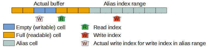
The ranges of the read and write indices are both twice the range of the indices in the actual buffer. This allows one to distinguish between completely full and completely empty buffers which with single-range design will also need one to keep the number of full cells in another variable, which requires updating two variables in each operation, requiring protection (by interrupt disable or a semaphore). Another way is the never-full pattern where the buffer is one cell longer than the size of the buffer. In this case that would be good also as the cells are small. If they are large then the alias indexing pattern is an alternative to the index-and-size one.
The FIFO module is used both in the PCF8576 emulator and the console to allow fast interrupt service along with potentially slow background processing.
The console
The console provides a 38400 baud serial channel for tracing, logging, and debugging, when one needs that during the FW development. With a real-time system using a debugger and single stepping is not an option. Even less with a design with limited amount of pins available. In this design the serial port shares the pins with the in-circuit programming the way hinted by the classical PicKit 2 serial port tool: UART chip to host on ICSPDAT (PGD) and host to chip in ICSPCLK (PGC) pin. Wonder why this very useful feature of PicKit 2 was never made available with PicKit 3 or 4.
The console provides basic putc and puts as well as single byte puth for dumping bytes in hex. The receiving direction provides single-byte get and buffer reading read interfaces.
bool_t console_int_handle(void)
{
    bool_t serviced = FALSE;
    if (PIR1bits.RCIF && PIE1bits.RCIE)
    {
        uint8_t c = RC1REG;
        if (fifo_put(&rx_fifo, c) == FAIL)
        {
            ++rx_fifo.n_fail;
        }
        serviced = TRUE;
    }
    if (PIR1bits.TXIF && PIE1bits.TXIE)
    {
        int16_t c = fifo_get(&tx_fifo);

        if (c < 0)
        {
            PIE1bits.TXIE = 0;
        }
        else
        {
            TX1REG = (uint8_t)c;
        }
        serviced = TRUE;
    }
    return serviced;
}
In both directions the background process reads or writes the FIFO, and the HW is handled by the interrupt processes. The transmit process uses the TX interrupt enable to start and stop the TX when the buffer is written or becomes empty, respectively. It is worth noting that in 8-bit PIC processors the interrupt flag is masked by the enable before passing the interrupt request to the core, so one must and the flag with the enable before deciding that this flag actually caused the interrupt. A thing easily forgotten.
The LCD module
This module implements the driver for a HD44780U-compatible character matrix module. The actual driver in the GTC-16026 module I used is KS0066. The initialization procedure for the 4-bit interface is incorrect in the KS0066 datasheet. It has always been. So whenever implementing the 4-bit interface use the procedure from the original HD44780U datasheet, to avoid the debugging of lost-display-after-reset issues.
This time I coded the pin-togging with a set or macros that create a kind of mini language. That is why the macros have the semicolons in them, a practice I otherwise abhor.
This module provides also a simple putc and puts interface for writing text to the display augmented with the ability to define the line and column of the writing. The module provides two special glyphs which are not a part of the normal character set of these modules. The thunderbolt glyph is used to show that the iron is heating. Even though in the display it is next to each of the sub displays of preset temperatures, only the one next to the rightmost sub display seems to be used. The other glyph is a lock icon shown in the right bottom corner when the temperature setting is locked.
The LCD emulator module wd1lcdemu
This module is arguably the most complex part of the FW. It contains a bitmap data data structure segments to keep the state of each segment in the LCD glass.
static struct segments {
    union {
        struct {
            uint8_t standby : 1;
            uint8_t setback : 1;
            uint8_t off     : 1;
            uint8_t offset  : 1;
            uint8_t window  : 1;
        };
        uint8_t value;
    } menu;
    union {
        struct {
            uint8_t deg_c  : 1;
            uint8_t deg_f  : 1;
            uint8_t min    : 1;
        };
        uint8_t value;
    } unit;
    union {
        struct {
            uint8_t f1     : 1;
            uint8_t f2     : 1;
            uint8_t f3     : 1;
            uint8_t lock   : 1;
            uint8_t remote : 1;
            uint8_t minus  : 1;
        };
        uint8_t value;
    } icon;
    segment_t A[3];
    segment_t B[3];
    segment_t C[3];
    segment_t D[3];
} segments;
The state of these bits is set by the wd1_set_seg() function called from the PCF8576 emulator when it detects a write to the segment state memory. The mapping of each bit in the memory to back planes and segment groups is simple (the glass is 1:3 multiplexed):
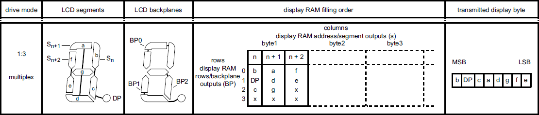
For simplicity the function passes one bit at a time, and hence is called eight times for each byte written to the display by the main controller. This isn't any less efficient than passing the whole byte, but it simplifies the interface and makes it more logical with respect to the actual HW connections between the controller and the glass.
The wd1_set_seg() function appears to be complex, but ti just maps the back-planes and segments to the required bits as is shown in the segment mapping:
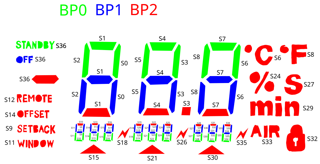
The logic of the mapping from this glass to the 16x2 character matrix is
// ===================================================================================
//      0    1    2    3    4    5    6    7    8    9   10   11   12   13   14   15
//   +----+----+----+----+----+----+----+----+----+----+----+----+----+----+----+----+
// 0 | M1 | M2 | M3 | M4 |    |    | N  | A1 | A2 | A3 |    | U1 | U2 | U3 |    | R  |
//   +----+----+----+----+----+----+----+----+----+----+----+----+----+----+----+----+
// 1 |    | B1 | B2 | B3 | F1 |    | C1 | C2 | C3 | F2 |    | D1 | D2 | D3 | F3 |LOCK|
//   +----+----+----+----+----+----+----+----+----+----+----+----+----+----+----+----+
//
// M1-4: Menu
// N:    Minus sign
// A1-3: Main digits
// B1-3: I digits
// C1-3: II digits
// D1-3: III digits
// U1-3: Units
// R:    Remote symbol
// F1-3: Thunderbolt symbols
// LOCK: Lock symbol
// ===================================================================================
//
// - Menu as rotating group of active segments
//     STANDBY    STBY
//     SETBACK    SETB
//     OFF        OFF
//     OFFSET     OFST
//     WINDOW     WIND
// - Units: only one active at a time, direct from the segment
//     <deg> C
//     <deg> F
//     min
// - F1-3 and LOCK: direct from the segment
// - Minus sign, Remote symbol, direct from the segment
// - Each 7seg group through interpreter
//     Digits and special digits OFF, FCC, FSE, Id, -1-, -2-
//     All other 7-seg combinations via special glyph.
// ====================================================================================
The interpretation of the bits to text in the matrix display is done by a state machine driven by the main event loop. The state machine updates the texts cyclically, one part of the display at a time, the parts being the menu indication on top left, unit on top right, single-character icons, and the four seven-segment groups.
As the menu may have multiple indications activated and the reserved space can display only one at a time, if more than one are active at a time the indications are cycled, 500 ms per indication. The units and icons are simple mappings.
The seven-segment groups are a bit more complex. A seven-segment pattern is coded to a 7-bit value which is then converted to the corresponding character by a table lookup. When the segments are being updated, there may appear odd patterns that are not actual intended letters or numbers. That would appear confusing if all patterns were encoded to something that resembles the segment pattern, or, as I considered, shown as actual corresponding 7-segment patterns created on the fly using the user-defined characters. Therefore I decided to indicate them by a special character * which means that the currently showing character should not be changed.
One small change to that logic was needed, as the seven-segment pattern for number 5 and letter S used in indication of restoring the factory settings result from the same pattern. Number 5 does not look great in F5E, so a logic of showing S instead of 5 when the character to the left is F took care of showing the nice FSE.
The PCF8576 emulator module pcf8576emu
The LCD controller emulator provides a buffer for the I2C writes and implements a state machine that interprets the the writes as commands and data and passes them to the LCD glass emulator.
The I2C module, in interrupt context, tells to this emulator when a write begins, because the bytes at the beginning are commands, until end of commands is indicated by a command that has the msb (continuation bit) zero.
For each received byte the state machine in the interrupt context interface puts to the FIFO two bytes. The first one indicates if the byte is command or data and the second one is the command or the data. This very simple splitting of the commands and data allows for the emulator state machine (in fact, not a state machine after all, as the state was moved to the interface) to pass the received bytes to command or segment data processing as needed.
The command byte handler handles only a subset of the commands. Those of no interest to this application are ignored. Some of the commands are even passed on to the LCD emulator but then ignored there as those functionalities, enable/disable and blinking, appear not to be used. So only the multiplexing and the data pointer setting are implemented. Even the banked memory is not implemented as this application uses 1:3 multiplexing and the banking works only with the 1:1 and 1:2 modes.
The segment states are passed to the LCD glass emulator when they are written so this emulator does not model the contents of the memory. It models only the by behavior of the data pointer and the byte-to-memory-bits mapping. According to the datasheet the PCF8576 does not appear to support read-back of the memory, so retaining the written data in the way allowing the read-back is not relevant.
The I2C module
The I2C driver is very simple, as only the receiving direction is needed. The HW is initialized to listen to the base address 0x70 of the device, no support for subaddresses. It is initialized to handle the receiving automatically. At 50 kHz clock rate the bytes can arrive at maximum of 5.56 kHz rate which means that at 8 MIPS rate the CPU can execute 1440 instructions per a byte. When accounting to the other facts that at maximum the main controller is sending 6 bytes of segment data every 10 ms but typically much less, that is 48 segment changes in 10 ms meaning there is 1666 instructions for each bit of segment data even in the worst case. Really much for getting everything done.
Of the many interrupts only the buffer-full (BF) and the end-condition (P) are enabled. The BF interrupt along with the knowledge whether data or address (D_nA bit) was received the received byte is passed to the PCF8576 emulator or the begin is indicated to it. Even the stop-condition indication is not actually used. It was used only in the testing phase to indicate the end of a write, but the same information comes from the D_nA indication of the address as the addressing phase means that previous transfer has ended, though that happens later.
Discussions
Become a Hackaday.io Member
Create an account to leave a comment. Already have an account? Log In.