Let's start with a broad overview of what we're dealing with.
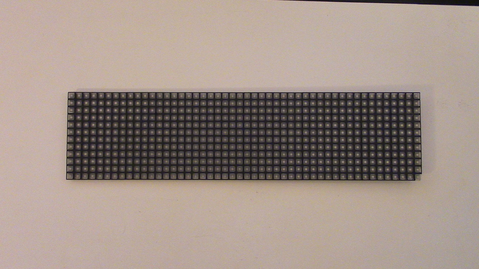
Each board has one one side a 48x12 array of RGB LEDs covered by a multi-part injection molded lens assembly composed of a frosted lens panel and six black grid panels that help visually separate the individual pixel squares. The fact that the black trim bits are 8x12 suggests they made modules of various sizes...
On the back of the board is two power connections, a 60-position main data connector, a step-down converter (as a separate assembly), a bunch of ICs and misc. passives. My boards are stamped "SACO TECHNOLOGIES V9 REV. B." with a field for a hand-written serial number that is blank.
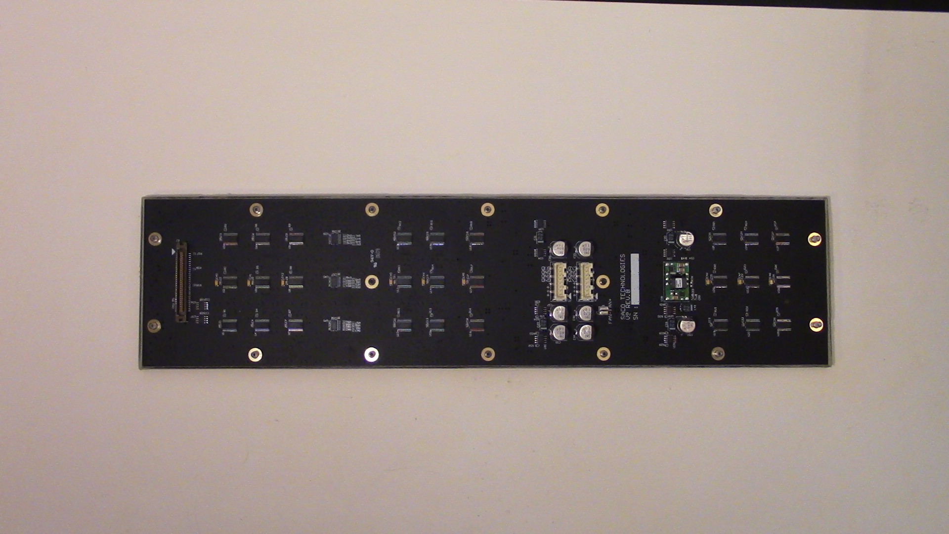
Power connectors are 8-pin, 2.54mm (0.100") pitch, with 4 pins each for +5V and GND. Not able to identify the part number (yet?). All the +5VDC and all the GND pins are connected to each other to form common rails. +5VDC feeds the DC-DC converter, all of the ICs (except the P-channel mosfets), and also connects to the +5V pins of the main data connector. Let this be a warning: It is possible to accidentally power the entire board through the pins on the main connector, which I really doubt are up to the task. In my testing I only connected the GND for common voltage reference and used only the bulk power connectors for the +5VDC supply.
The main data connector looks to be a 3M "Pak 50" series, P50L-060P-AS-DA. The mating connector is P50L-060S-AS-DA. At time of writing, the plug that matches the socket on these boards goes for $10.52 each on Digikey, with a minimum order of 200 and 28 weeks lead time, so we ain't doin' that.
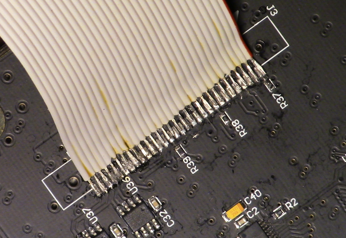
An old floppy drive cable fits the 1.27mm pitch perfectly. This soldering job might not look like much, but it's worth at least $2,104. (and 7 months...)
The power supply module, which steps the 5VDC supply to 3.3VDC, is a PTH05060. This module is rated for an output of 10 amps at a configurable 0.8 to 3.6VDC. As far as I can tell, this 3.3VDC rail is used exclusively for the red LEDs, and all the other LEDs and ICs are supplied by the 5V rail.
The rest of this chips include: LED drivers, octal buffers, mosfet drivers, and dual P-channel mosfets. There are a total of 27 LED drivers, which of course are the key to the whole thing, but let's cover the other ICs briefly.
There are three VHCT541 octal buffer chips, all with their output enable pins tied to ground. 24 of the 28 data pins from the main connector go to these buffers, and since the output is always enabled they immediately pass the input pin state to the output pins. I presume this is done to save the controller from having to source current to drive so many LED driver lines.
Four of the data pins from the main connector go to two dual-channel MOSFET drivers, TC1427C, which of course drive the P-Channel MOSFETs at the other end of the board. Each control input controls 4 of the 16 MOSFETS.
There are eight dual P-Channel MOSFETs. Mine are labeled "D6P02." These are divided into four ICs for the 5VDC rail and and four ICs 3.3VDC rail, but are connected in parallel on their respective rails. That's two MOSFETs per rail per input, and they are in different chips presumably to spread the current out and reduce heat load.
And now the 27 LED drivers; Texas Instruments TLC5941 (Datasheet). These are arranged in three groups that I'll refer to as "banks" in keeping with Huffine's post. Each bank is divided into three "rows," and each row is powered by four power rails each switched separately by the MOSFETs (A,B,C,D)
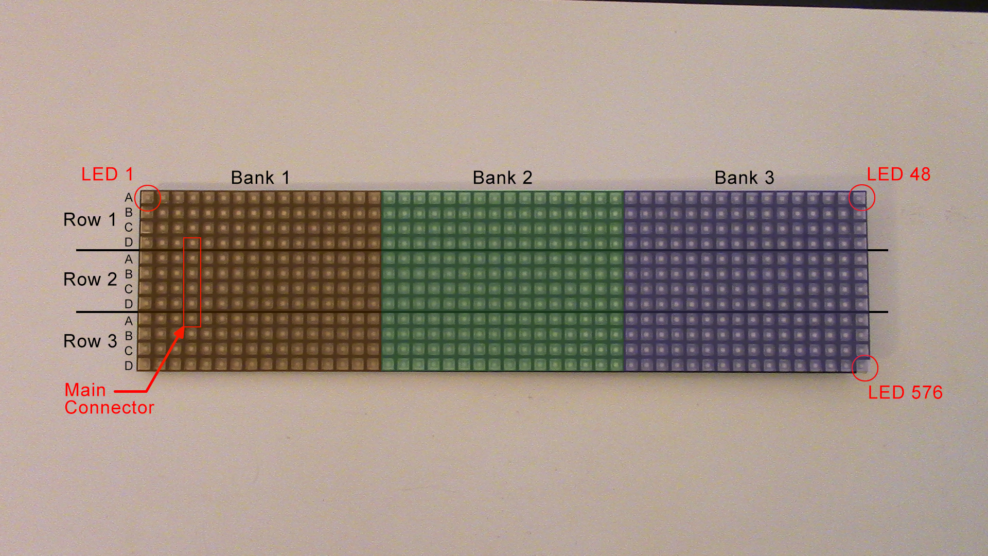
9 drivers per bank, 3 per row. Each driver in a row's group of 3 does R,G, and B channels. It's important to note that they are electrically grouped by color, meaning you will need to separate the pixel data by color channel and clock in three rows worth of data for each color, rather than clocking in one row of RGB data.
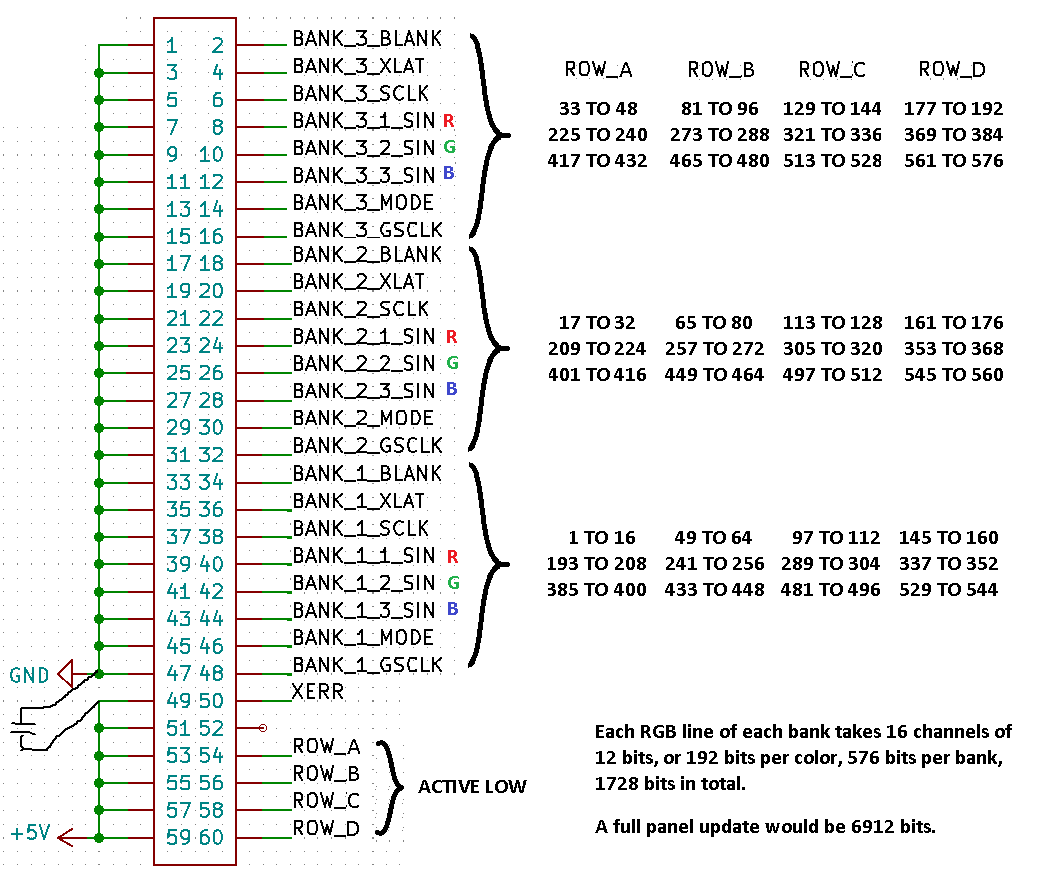
A modified and annotated pinout from Huffine's post. They had originally had Banks 1 and 3 reversed, so I changed them around to that LED1 was in Bank 1, Row 1.
That pretty much covers the whirlwind tour of the physical construction, and is more than sufficient to get us started on the main task of figuring out the data format and devising a driver scheme...
Discussions
Become a Hackaday.io Member
Create an account to leave a comment. Already have an account? Log In.