There is a fair bit to the I/O side of this machine. I had planned on doing a log entry once the I/O was done but it's taking a while so let's do an update now.
There are six facilities to the Rack8 machine's I/O:
- The Keyboard
- The Bank Latch
- The Memory Mode Latch
- The Debug Latches
- The Omniport
- The System Latch
Currently the first four are up and working while the Omniport and the System Latch are next in line for implementation. So what are these things, and what are they for?
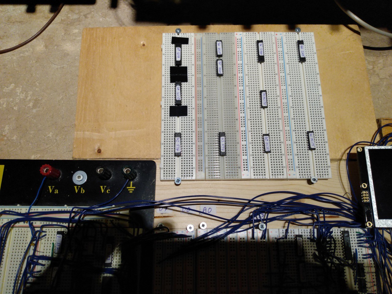
But before we launch into the details, a couple of photos. The breadboard version of Rack8 is built on a piece of wood to which are attached the solderless breadboards. But the board was full and now it was time to implement I/O. So I literally glued another piece of wood onto the top of the existing wood, attached more solderless breadboards, and populated it with the proposed I/O chips. Photo, as of two weeks ago, here:
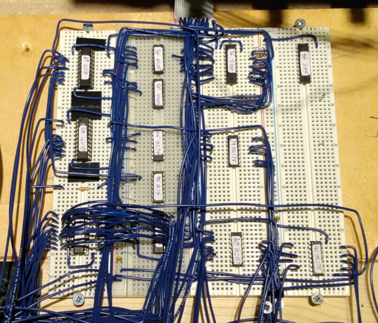
Now with much of the I/O working it looks like this:
while the whole project now looks like this:
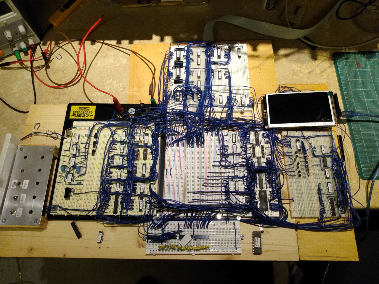
with the I/O section way up at the top. Note the 20 conductor ribbon cable at the very top which goes off to the keyboard.
The schematic for the implemented-so-far IO can be found here.
Behind The Scenes...
There are two GAL chips, upper left corner in the schematic, that generate the pulses to clock the various IO devices and any other signals needed. The logic equations for those GALs can be found here and here.
The Keyboard
It's kind of obvious what this is for but the way it is implemented in the MCM/70 and hence this machine is interesting. Unlike most microprocessors, the 8008 I/O-READ instruction is actually a WRITE-READ operation. Yup, a single instruction can both write and read at the same time. During a READ operation the content of the accumulator is presented on the low 8 bits of the address bus while the data to the processor you need to present on the data bus.
The MCM/70 took advantage of this when reading the keyboard. The keyboard itself is just an X-Y matrix of keys; no chips, no diodes, just the keys. To scan the keyboard the CPU does an IO-READ operation wherein - on the WRITE side of things - it sends one bit to the X part of the matrix and - on the READ side of things - sees what comes out from the Y part of the matrix. By probing all eight possible WRITE bits you can which key is down, or if none are down.
In the schematic the components for the keyboard start in the middle and then move diagonally to the upper right. In the middle U34 and U34 - open drain inverters - send the bits from the address bus to the keyboard which is connected to J5. What comes back from the keyboard is gated onto the data bus by U36. Because it's driven open drain, the pullup resistors RN5 keep any undriven lines high. Part of the reason that it's driven open drain is that the keyboard, like the original MCM keyboard, has no diodes so open drain keeps things from shorting if the user presses more than one key at a time.
The Bank Latch
Like the MCM/70, this machine has 16 banks of 2K each at address X'1800'-X'1FFF', and only one bank at a time can be active. A 4-bit latch, set by IO write instruction X'51', selects the current bank. In the schematic the Bank Latch is over on the right side in the middle. Nothing exciting here although - brain fade alert - I initially had the input to the bank latch connected to the data bus. You get data from the data bus, right? Well not on this machine you don't. Took me a bit of debugging to figure that out, then we had a DUH moment, followed by some rewiring. Then it worked..
The Memory Mode Latch
As discussed in the Real Memory log post, there are four bits that control the mode in which the Rack8 memory works at any given time. In the schematic U41 is the 4-bit latch that actually provides the bits. When the machine is running, the memory mode can be changed by issuing an X'59' I/O instruction. In that case, the data for the latch comes from the address bus via U40, a quad 2-to-1 multiplexer. But when the machine is reset, then the mux supplies the bits from four switches, so that the machine can be placed in a known memory mode at reset time. The PINT signal ("processing interrupt") is high when an interrupt, aka reset, is in progress which tells to mux to supply data from the switches.
The Debug Latches
On the original rack machine we had a software debugger which allowed us to set breakpoints, to view and change registers and memory, and to trace instructions one at a time. In order to do that the debugger had to be able to save and restore the state of the machine. But, unlike later microprocessors, the 8008 is incapable of saving its own state. In particular you need to save the registers. The obvious place to save the registers is in memory. But in order to store a byte in memory you have to load the H and L registers with the address of the memory, in the process wiping out the values in the H and L registers. Fabulous. So to solve this problem, the debug latches are a pair of one-byte registers which can be written and read using an I/O instruction. Fortunately I/O instructions don't alter the condition codes.
Note that the debug latches, like the keyboard, make use of the WRITE-READ capability of the 8008 READ instruction. When clocked, the old value is presented to the data bus while the new value is captured from the address bus. It's quite handy.
Thus, to save the state of the machine, the drill is:
- Read debug latch 0. That puts the value from the A register into debug latch 0, thus freeing up the A register. It also gets you the value that was previously in debug latch 0 but right now we don't care about that.
- Copy register L to register A and sent it to debug latch 1.
- Copy register H to register A.
- Load the address of the register save are into H and L then save the registers.
Next you need to save the condition code. The 8008 also has no good way of getting those so you just do various tests and note the results. Technically the condition codes are output on the data bus during the T4 cycle of memory cycle two of an IO read but doing anything with that would involve yet more hardware; a bit of software is rather less work.
On the schematic the debug latches are on the left, just under the GALs.
Restoring the state of the machine is pretty much the reverse of the above. The 8008 has no way of restoring the condition codes directly; instead, based on what you want them to be, you need to do some fancy dancing in software but it is possible.
The Omniport - implementation in progress
The omniport is the bidirectional I/O bus by which all external peripherals (e.g. printer, floppy disk, card reader, RS232 interface etc.) communicate with the MCM/70.
The System Latch - implementation in progress
The MCM/70 needed to be able to receive and send a few bits of "system" information. In particular it received a signal from the power supply saying if mains power had been lost. In that case, the machine would if possible save the content of memory to cassette tape and then do an orderly shut down. It was like "suspend to disk" long before that became a popular option. It also needed to be able send a signal to the power supply telling it to shut off.
Discussions
Become a Hackaday.io Member
Create an account to leave a comment. Already have an account? Log In.