 Steph
Steph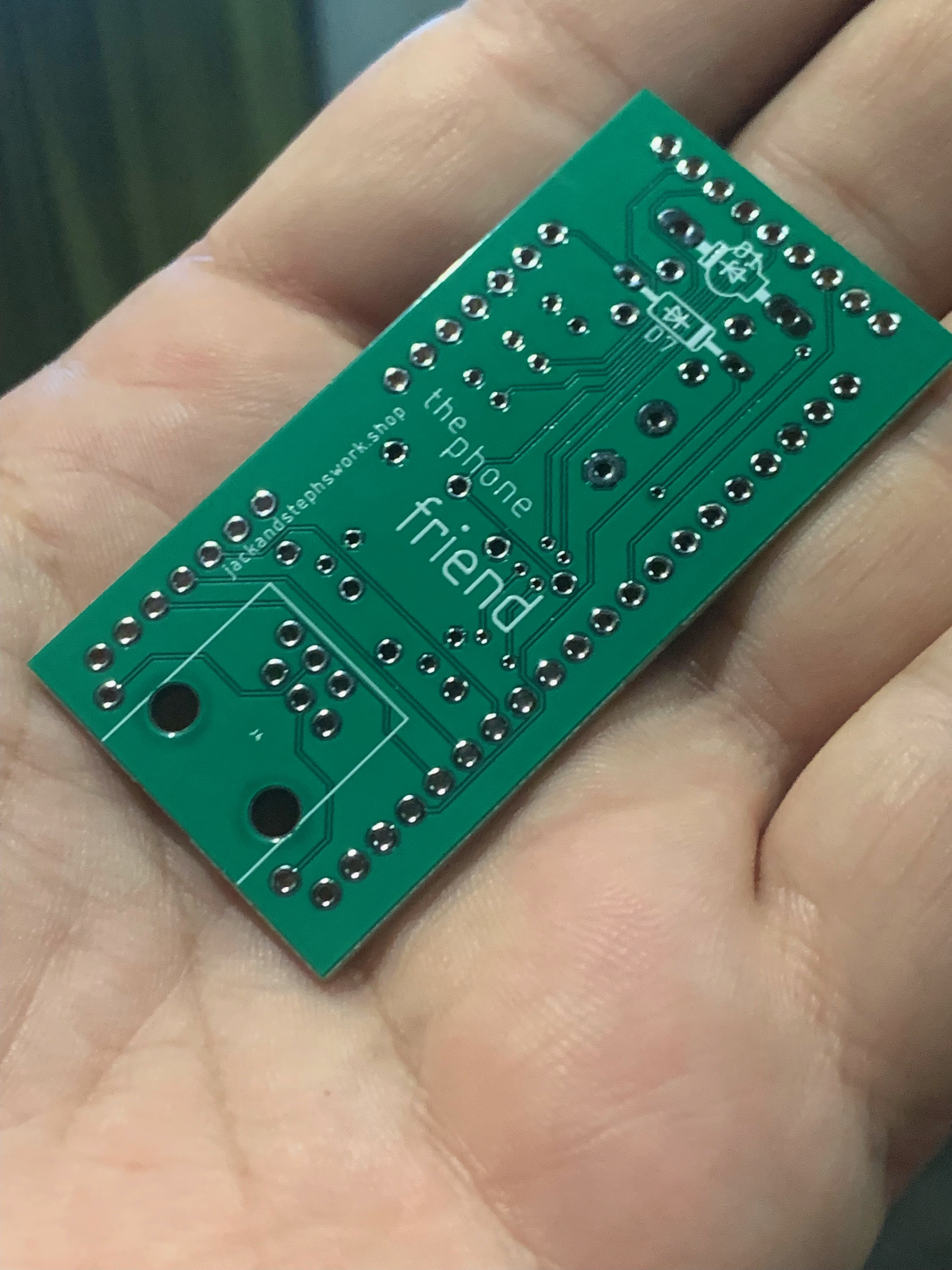
Look I Made a PCB!
It's my first one!
It went relatively well! I soldered the AG1171 and a Pi Pico W to the board, and the attached phone rang on the first try:
I felt proud when it worked because my expectations for this first board were very low. I didn't even expect all the parts to physically fit together. But they did! The handset audio also worked, but it sounded noisy and distant. It was a pretty cool effect actually, sounding rather similar to a long distance phone call over a bad connection.
But I knew something was wrong.
A closer look revealed that I had routed the audio to the wrong pins. Somehow, enough signal leaks out of a neighboring pin (which isn't supposed to be connected) to make a lo-fi version of the audio output. I re-soldered the decoupling capacitors to the correct pins, and the audio came through to the handset crystal clear. Well, crystal clear for a phone, anyway. I'll have to fix the routing issue in the next version of the board, but I'll also keep in mind the accidentally discovered lo-fi option. Depending on the outcome of some tests, I might build in a switch to select between the two.
Zero to hero
Since I didn't know any of this stuff two weeks ago, here's some basic info about designing a PCB.
The design consists of two parts, the schematic and the board. The schematic is basically a map of every component that will be on the board, and the connections between each component. The Phone Friend's schematic looks like this:
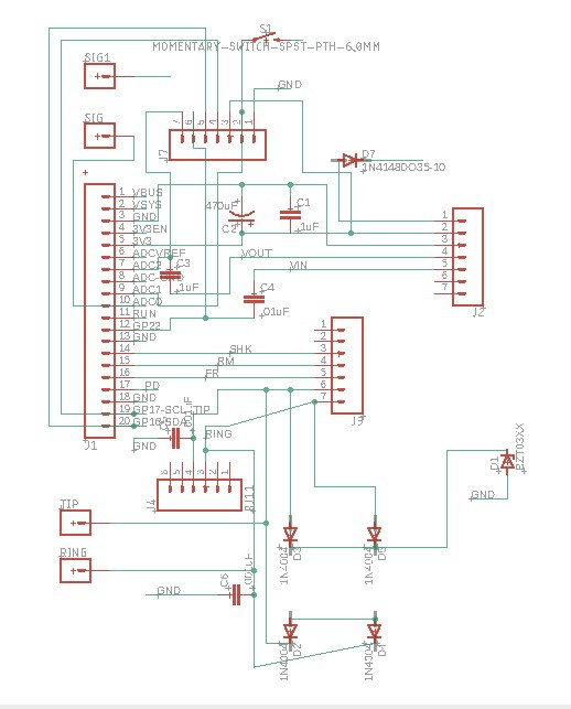
- be aware that this initial version is sloppy and contains errors, so don't try to follow it.
Once the components are placed and connected in the schematic, they can be positioned on the board. The board design describes the physical placement of the components and the copper traces that will connect them. This is the description of the PCB that will ultimately get manufactured. It's not unlike a photoshop file with multiple layers. One layer designates the outline of the board, another layer marks the holes to be drilled, and other layers represent the copper traces on both the top and bottom side of the board, the pads, the silkscreen layer for the printed labels, etc.
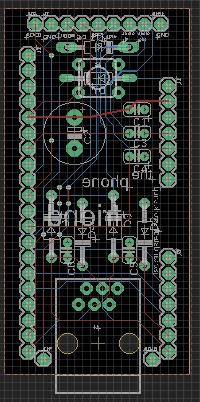
The board I designed carries the AG1171 and the Pi Pico W, along with a handful of mostly optional additional components. It simply routes power to the AG1171, as well as control and audio pins to and from the Pico.
The board also carries a standard telephone jack, which is technically called a RJ11 connector. It's the large rectangular shape at the bottom of the board in the graphic above. The six green circles inside the top of the rectangle are holes for the pins of the jack, and the two larger holes beneath simply accept plastic mounting posts that help hold the jack in place. Since we only care about connecting to the phones tip and ring lines, we will only utilize the two middle pins of the connector. That means our jack is fully described as a RJ11 6p2c, where the "6p" portion describes the number of possible connectors and the "2c" describes how many connections are actually in the connector.
Which brings us to...
The Wonderful World of Part Selection
So far our PCB exists only virtually, but later it will have to match up rather exactly with the physical properties of the parts we'll eventually solder onto the board. Many (all?) of the parts you can put on a PCB come in a variety different shapes and sizes called their "package." Once the package is chosen, a matching part is added to the schematic, hopefully with the correct footprint for the package.
There are two ways to add parts to your schematic:
- Find the part in a library
- Build the part yourself
#2 sounds hard so I stuck to finding parts in a library that somebody else already built. I found all the parts I needed in a library provided by Sparkfun.
In the case of the RJ11 phone jack, I used the RJ11 part found in the Sparkfun library. Technically, this footprint has more holes than we need, but as stated above, it seems like a lot of work to customize the part, so I went with the library version, unmodified. Additionally, I didn't want to purchase the matching part from Sparkfun because of those same extra connectors (and price). So, I took a gamble and ordered a few different jacks from various suppliers. When my PCB arrived, I found that all the jacks I ordered fit correctly, with the same footprint and the same pin positions.
With other components, I wasn't as lucky. The capacitors I chose from the Sparkfun library, for example, turned out to have very closely spaced through-holes in the footprint compared to the pin spacing of the capacitors I actually bought. The leads on the capacitors are plenty flexible and long enough that I can still attach them, but it doesn't look very good. In the next version, I'll find a library part with a wider footprint.
The same goes for almost everything on the board- in the next version, I'll do something a bit different. I've spotted many minor issues that became obvious only when holding the manufactured board. I've also spotted major issues about how the big chips like the AG1171 physically fit next to the other stuff around them. Nearly everything will move or change or switch sides in the next version, hopefully resulting in a correctly routed board with a better fitting yet more compact arrangement of parts. And maybe some LEDs, just for fun.
Discussions
Become a Hackaday.io Member
Create an account to leave a comment. Already have an account? Log In.