 NNNI
NNNIIntegrating ADCs fall under the broad category of ADCs that convert voltage to time, which include voltage-to-frequency and voltage-to-duty cycle. The name itself implies that the mathematical function of integration takes place along the conversion process. The most convenient electronic building block to perform that task is the capacitor, the voltage across which is an integral of the input current over time, described by:
Since an integrator is basically a first-order RC filter, most of the high frequency noise on the input is filtered out, leading to cleaner readings. On the other hand, the integrating action also means that conversion times are relatively slow.
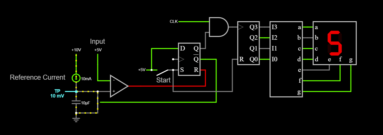
The simplest manifestation of an integrating ADC is the single-slope ADC, which consists of a current source feeding a capacitor, a comparator and some controlling circuitry. The input signal is fed into one input of the comparator, and the current source driven capacitor is connected to the other. External circuitry maintains the capacitor at 0V through a shorting switch. When the conversion starts, the shorting switch is opened and the capacitor charges through the current source. Since the charging current is constant, the voltage ramps up linearly. When the voltage across the capacitor equals the input voltage, the comparator signals the control circuitry to stop the conversion. It also shorts capacitor to reset it for the next cycle. The actual conversion from analog to digital takes place at the comparator output, which is a binary representation of the state of charge of the integrating capacitor. This is used to gate a series of clock pulses. The number of pulses is directly proportional to the voltage on the capacitor, and therefore the input voltage.
Here's a link to a Falstad simulation.
Although straightforward, this simplistic method is not without its flaws. Integrating ADCs rely heavily on the integrating capacitor being stable with time and temperature. There is one other undesirable property of capacitors that can affect linearity - dielectric absorption. Increasing precision also places demands on the comparator, which needs to have a low offset voltage and low input noise. Although the absolute value of the offset voltage can be calibrated out, its variation with temperature is harder to account for. Input noise also affects the repeatability of the comparison. The latter effect is practically never mentioned in datasheets and determining it can be trickier than that of op-amps.
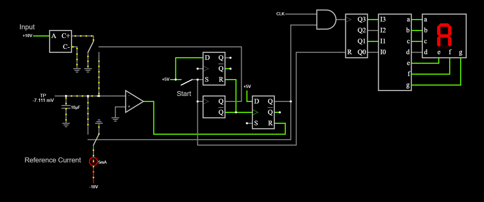
Dual-slope ADCs solve both of these problems to a large extent. A current proportional to the input voltage is allowed to charge the integrating capacitor for a fixed time period. The voltage on the capacitor after this time is proportional to the input voltage. The capacitor is then discharged through a constant current source. The discharge time is proportional to the input voltage and can be digitized in a similar manner as the single-slope.
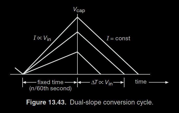
(The Art of Electronics, pg. 915 Figure 13.43)
The above diagram from The Art of Electronics explains the dual-slope conversion process.
Since the process now involves two slopes - one to charge the capacitor to a voltage proportional to the input voltage and the other to discharge it down to zero - the effects of dielectric absorption are seen on both slopes and have a smaller effect on the readings. Since the slopes start and end at the same voltage, comparator offset cancels out.
Here's another Falstad simulation of a dual-slope ADC.
The limitations of dual-slope ADCs occur at the higher and lower end of the measurement range. At the lower and, resolution is limited by measurable integrator swing, clock resolution and the noise floor. At the upper end, the integrator needs larger output swings for the larger input voltages, risking saturation. Another subtle disadvantage the dual-slope shares with the single-slope is that measurement time is proportional to the input voltage. In many cases, a constant measurement time is desirable.
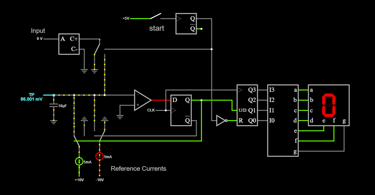
So far, the simple examples above contained only one reference current source. With the addition of a single reference current source of the opposite polarity, a multislope ADC can be created. The "multi" in multislope surprisingly does not refer to having multiple current sources/sinks of different values and thus leading to different slopes on the integrator, but to the fact that the two reference slopes are switched alternatively into the integrating capacitor. *
And here's yet another Falstad simulation of a multislope ADC.
The multislope ADC can be thought of as a simple triangle wave oscillator. Assuming zero input voltage and matched reference currents, the output of the integrator is a triangle waveform and the output of the driving flip-flop is a signal with a 50% duty cycle. Compared to the single- and dual-slope ADCs, the multislope is easily clocked. This means each clock cycle injects a fixed positive or negative charge into the integrator.
The input current, once switched into the integrator, causes an imbalance in the charge and discharge currents, and therefore changes the duty cycle of the oscillator. The loop now has to clock charge into the integrator to cancel out the input current. Over a large number of clock cycles, the difference between the amount of positive and negative charge clocked into the integrator is proportional to the input voltage. Even small currents trickling into the integrator over a long time can cause a measurable difference in the positive and negative counts, making this method suitable for measuring very small input voltages.
This continuous charge balancing method is no longer limited by integrator saturation, thanks to being in a closed zero-seeking loop. The integrator can now accept input charge indefinitely, provided the input current does not overpower either reference currents. Constant measurement time can also be achieved by integrating over a fixed number of clock cycles.
A natural extension of this technique is the delta-sigma ADC. I don't fully understand the math behind it, so it's safe to say it's beyond the scope of this project, although with the right number crunching it can still be implemented using the same circuit.
*An interesting side note: the legendary HP/Agilent/Keysight 3458A DMM does have multiple rundown slopes that are switched in, in decreasing slope order to speed up residue measurement.
Discussions
Become a Hackaday.io Member
Create an account to leave a comment. Already have an account? Log In.