 electronicsworkshops
Introduction
A Buck Converter is a type of DC-DC converter that can step down (i.e., reduce) a higher voltage to a lower voltage. It is a popular choice for power electronics applications because it is efficient and relatively simple to implement.
Buck Converters are commonly used in a variety of applications, including power supplies for computers, mobile devices, and LED lighting, as well as in automotive and industrial applications. They are known for their high efficiency, small size, and low cost.
Full project link :
https://electronicsworkshops.com/2023/04/16/how-to-design-own-buck-converter-12v-5v/
Working Principle of Buck Converter
The working principle of a Buck Converter involves the conversion of a higher voltage to a lower voltage through a series of switches, inductors, and capacitors. The basic operating principle of a Buck Converter is as follows:
The input voltage is connected to a switch (usually a MOSFET), which is controlled by a control circuit.
When the switch is closed, the input voltage is applied across the inductor, which starts to store energy in the form of a magnetic field. When the switch is opened, the stored energy in the inductor is released, and the energy is transferred to the output capacitor and load.

The output voltage is regulated by adjusting the duty cycle of the switch. The duty cycle is the ratio of the time that the switch is closed to the time that it is open.
By varying the duty cycle, the output voltage can be maintained at a constant level, even when the input voltage or load changes.
Overall, the Buck Converter works by converting the higher voltage input to a lower voltage output by controlling the switch’s duty cycle to regulate the output voltage. This results in an efficient, cost-effective, and reliable power conversion solution suitable for a wide range of applications.
Switching regulator (TPS54331)
The most important component in our design is Switching regulator (TPS54331).
We have selected this driver chip because due to its easy availability wide input range and has integrated mosfet.
It has 3.5-V to 28-V Wide Input voltage Range.

- BOOT: Connect 100nf capacitor between boot and sw pin.
- EN: Float the EN pin to enable.
- VSENSE: Connect to output voltage with feedback resistor divider.
- SS: It is slow start pin. The external capacitor is connected to this pin set the output rise time.
- GND: Ground pin
- VIN: Input supply pin
BOOTSTRIP CAPACITOR
The N-ch MOSFET for the high-side switch requires a gate voltage of VIN+ Vth (threshold voltage of the N-ch MOSFET) or higher. A step-up circuit is required because the gate voltage is higher than VIN. This circuit is configured with an internal diode and an external bootstrap capacitor (charge pump type).

The voltages on the SW and BOOT pins in the example of Figure 1 are described as shown in Figure 2, where Vf is the forward direction voltage of the built-in diode.

When the SW voltage is low during the switching operations in Figure 2, the electric charge is stored in the capacitor from VIN, thus resulting in the voltage of VIN-Vf across the capacitor. When the SW voltage is high, the BOOTvoltage increases up to 2 × VIN-Vf, and the built-in diode maintains the voltage at 2 × VIN-Vf. Therefore, the BOOT voltage switches between VIN-Vf and 2 × VIN-Vf
OUTPUT VOLTAGE SET POINT(VOLTAGE DIVIDER)
The output voltage of the TPS54331dr device is externally adjustable using a resistor divider network.I this divider network is comprised of R1 and R2. Use Equation6 and Equation7 to calculate the relationship of the output voltage to the resistor divider.
vref=0.8v

Schematic of 12v to 5v buck converter

Bill Of Material

Bill Of Material
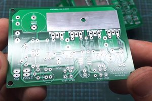
PCB Design

3D Design

Final Product

Manufacturing Files
Gerber Files
Bom Files
I have...
Read more »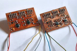

 mircemk
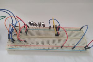
 Electroniclovers123