The power management PCB was designed with EasyEDA and ordered from JLCPCB. Initially, we considered using Altium to design the PCB. However, the startup and learning time required to use Altium proved too long for the timeline of our project.
We designed, ordered, and implemented one iteration of our PCB. If we had more time, we would have completed a second iteration. However, the tight timeline of the project did not allow for this.
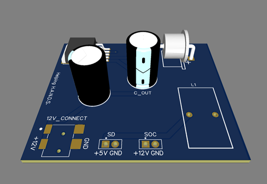
The purpose of the PCB is to provide regulated 12 Volt and 5 Volt outputs at a maximum of 3 Amperes. The servo driver and the ESP32 receive a 5 Volt input. The board also supplies a 12 Volt output due to a previous component, which is no longer included in the project. A 12 Volt regulated input is applied to the board through a barrel jack. To supply this power, a 12 Volt wall regulator is used to step down and convert the wall power to a DC signal. A buck converter is used within the PCB to step the 12 Volts down to 5 Volts. The PCB has 57.8 x 48.5 mm dimensions and is implemented on two layers.
As mentioned above, the PCB was ordered from JLCPCB for $21.71, of which $12.21 was shipping costs. Manufacturing of the PCB took two days, while shipping took seven days. Assembly took one day. Components for the PCB were either ordered from Digikey or sourced from our university's makerspaces and various student teams.
For PCB routing, we first used the auto-route feature from JLCPCB as a starting point, which we modified to eliminate as many 90-degree bends as possible. The trace width on our PCB is 1.5 mm, and the copper thickness is 1oz/ft2.
Power Analysis
Prior to designing the power management PCB, power analysis had to be done to understand the requirements of the board. The PCB is used to power the ESP32 as well as the servos. Both of those components require 5 Volts. However, the board also supplies 12 Volts. The largest current sink in our system is the servo bank. To understand the current draw of the servo driver, we tested actuating different numbers of servos at different speeds and noting the maximum values. During nominal operation, not all the servos will be moving at once, and they will be moving at a slower, steady pace. However, the servos will be under load from the hand. The estimated nominal current draw should not exceed 1 Ampere. When testing, the maximum current draw was 2 Amperes when all servos actuated simultaneously at maximum speed.
According to the above analysis, the PCB was designed for a system operating at a nominal 2 Amperes. To ensure our system is robust, an FoS of 1.5 was included. This means that all of our components were selected with a maximum current rating of at least 3 Amperes.
PCB Trace Width and Power Dissipation
The trace width for the power management PCB has to be able to withstand 3 Amperes. A trace width calculator was used to calculate the width for a 1 oz/ft2 copper thickness based on the 3 Ampere capacity. The calculator gave a result of 1.37 mm, and 1.5 mm was used in our design, giving an FoS of 1.1.
Power dissipation was also a factor in designing the PCB. The buck converter steps down 12 Volts to 5 Volts at a maximum nominal current of 2 Amperes. Therefore, the maximum nominal power dissipation is given by the equation below:
We chose a buck converter with thermal shutdown and current limit protection to dissipate this amount of power safely.
As well, the PCB has one via. A via calculator was used to verify the voltage drop and power loss in the via. Our via has a diameter of 0.8mm, with a length of 1.6 mm (the PCB's thickness). With a plating thickness of 1 oz/ft2, the voltage drop is 0.000993 Volts, and the power loss is 0.00298 Watts.
Discussions
Become a Hackaday.io Member
Create an account to leave a comment. Already have an account? Log In.