 Kuba Sunderland-Ober
Motivation
I wanted a basic 4.5 digit milliohm meter, for battery operation, designed to be affordable and use common, inexpensive parts, with some flexibility there: higher-cost part substitutes will perform better.
Op-amps and comparators figure prominently in the design and implement most of its functionality.
The design was prompted by and is a "reply" to Electrolab's milliohm meter project in the following video: Monte um Milliohmimetro super preciso!!! YouTube video. It demonstrates similar or better performance using jellybean general-purpose parts that were available in the late 1970s (save for the digital display), from a much lower supply voltage.
It is a stepping stone for a future project.
Requirements
- 3V to 5V operation,
- bare bones BOM cost around $15,
- reasonable accuracy with jellybean parts,
- 1Ω full-scale single range with some overrange capability,
- 4-wire operation only,
- zero- and scale factor (gain) adjustments,
- digital display with 1mΩ or better resolution,
- power supply monitor/indicator,
- 1V/Ohm analog output for e.g. data logging
- four op-amps (two duals), two comparators (one dual)
This is a Prototype!
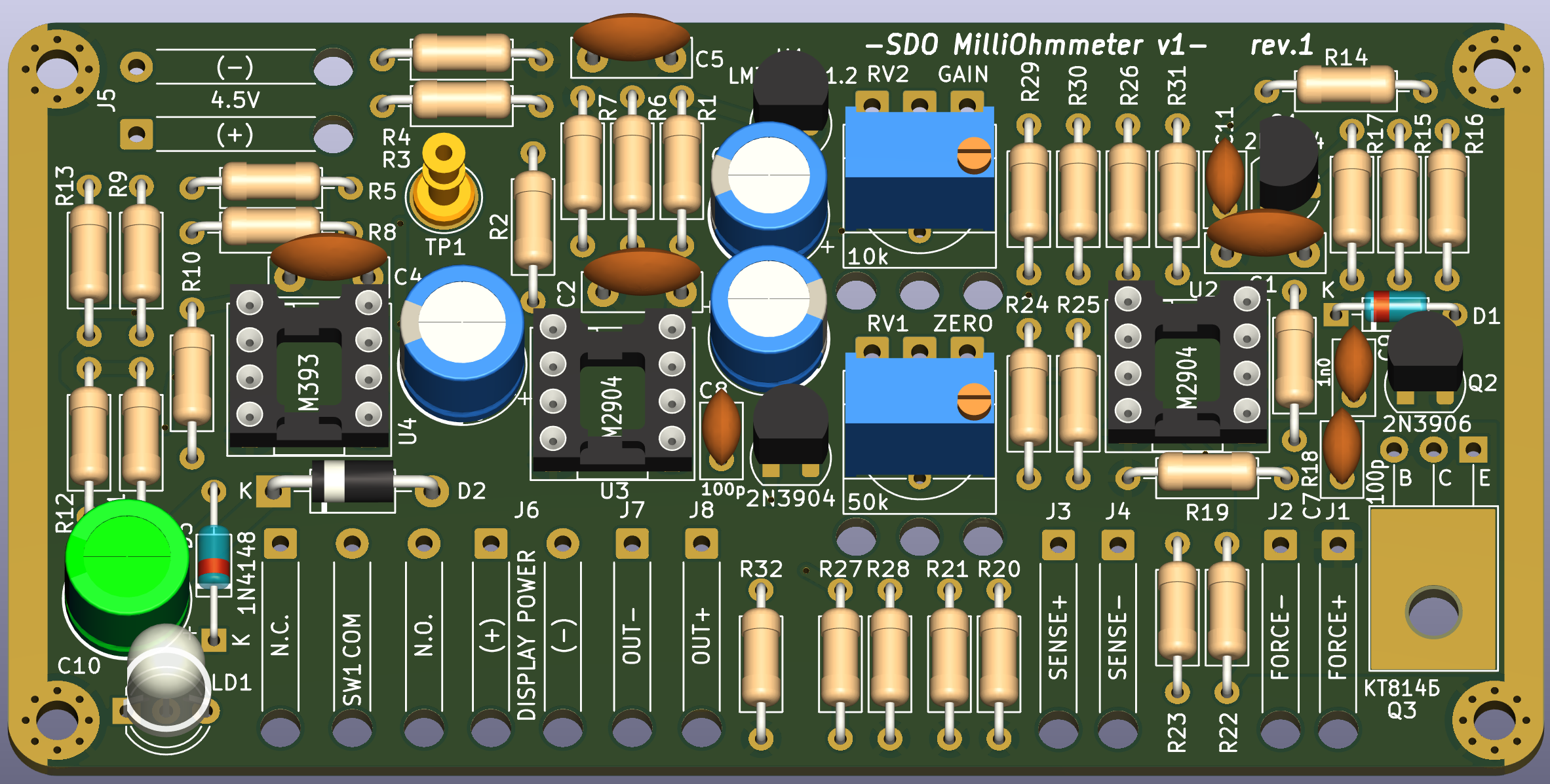
The design as shown suffers from problems not unknown to those who build a new design for the first time. My first mistake was to lay out the PCB based on the box dimensions from the eBay listing. Those dimensions turned out to be a bit of a "ballpark". The board dimensions should be 100x49mm to ensure fit.
The PCB is too wide by 1-2mm, and had to be sanded down to fit between the front and back plates of the enclosure.
The wire stress relief features are somewhat big for the wires used.
There's no provision for 2-wire measurement even though it would have been a reasonable requirement to have.
I've bought the PCBs from PCBWay, without any sponsorship. I am very happy with the quality so I can gladly recommend their "5 for $5" product. The size of the boards is limited to 100x100mm for that price. Larger boards cost more.
The laser-cut panels were ordered from Ponoko, without any sponsorship. Again, they provide high-quality product and I can recommend their service based on this experience.
Enclosure and Controls
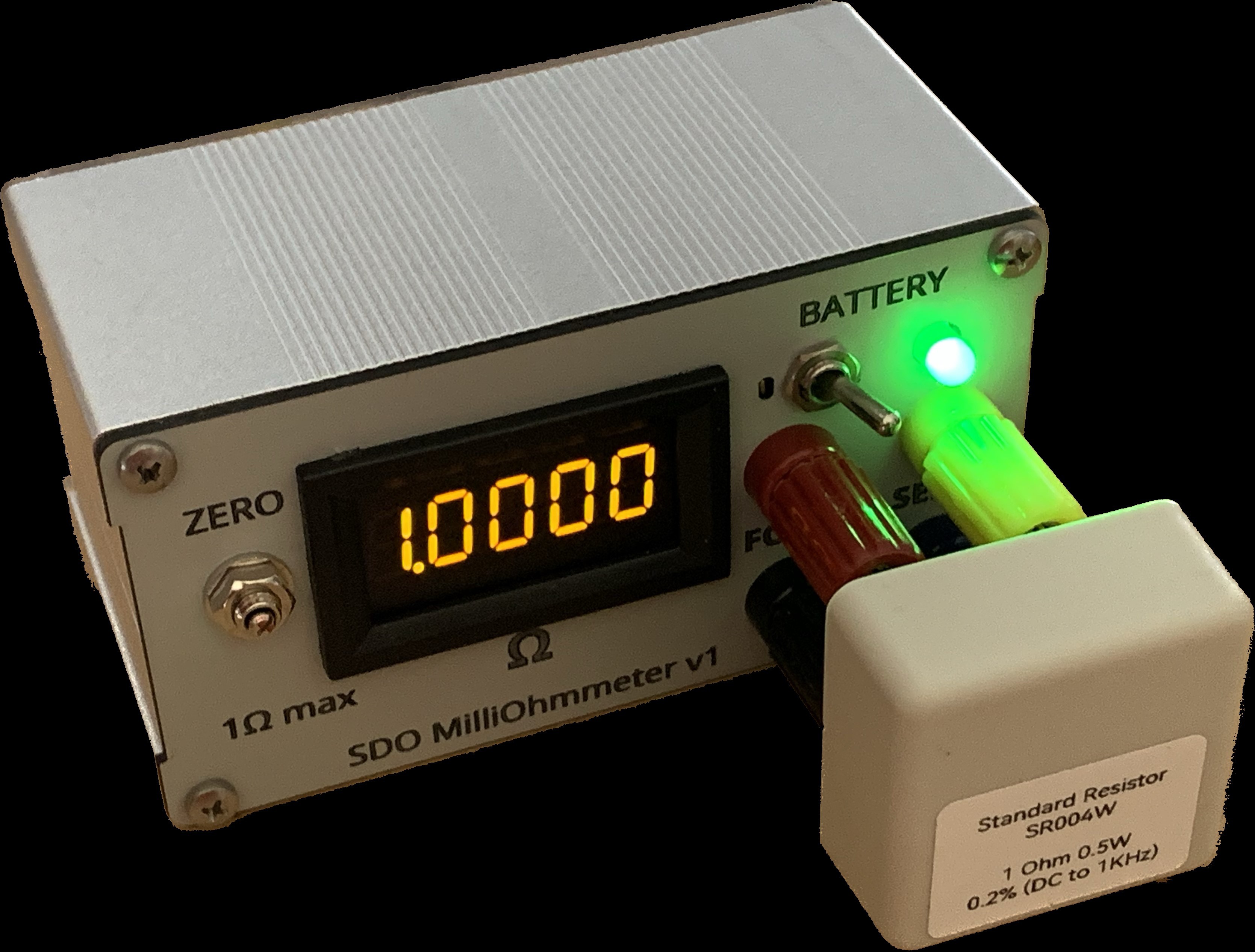
The meter is packaged in a two-part extruded aluminum enclosure. On the front, there are:
- a 4.5-digit resistance display,
- power switch,
- tri-color battery voltage indicator,
- force and sense binding posts (jacks),
- a zero adjustment trimmer.
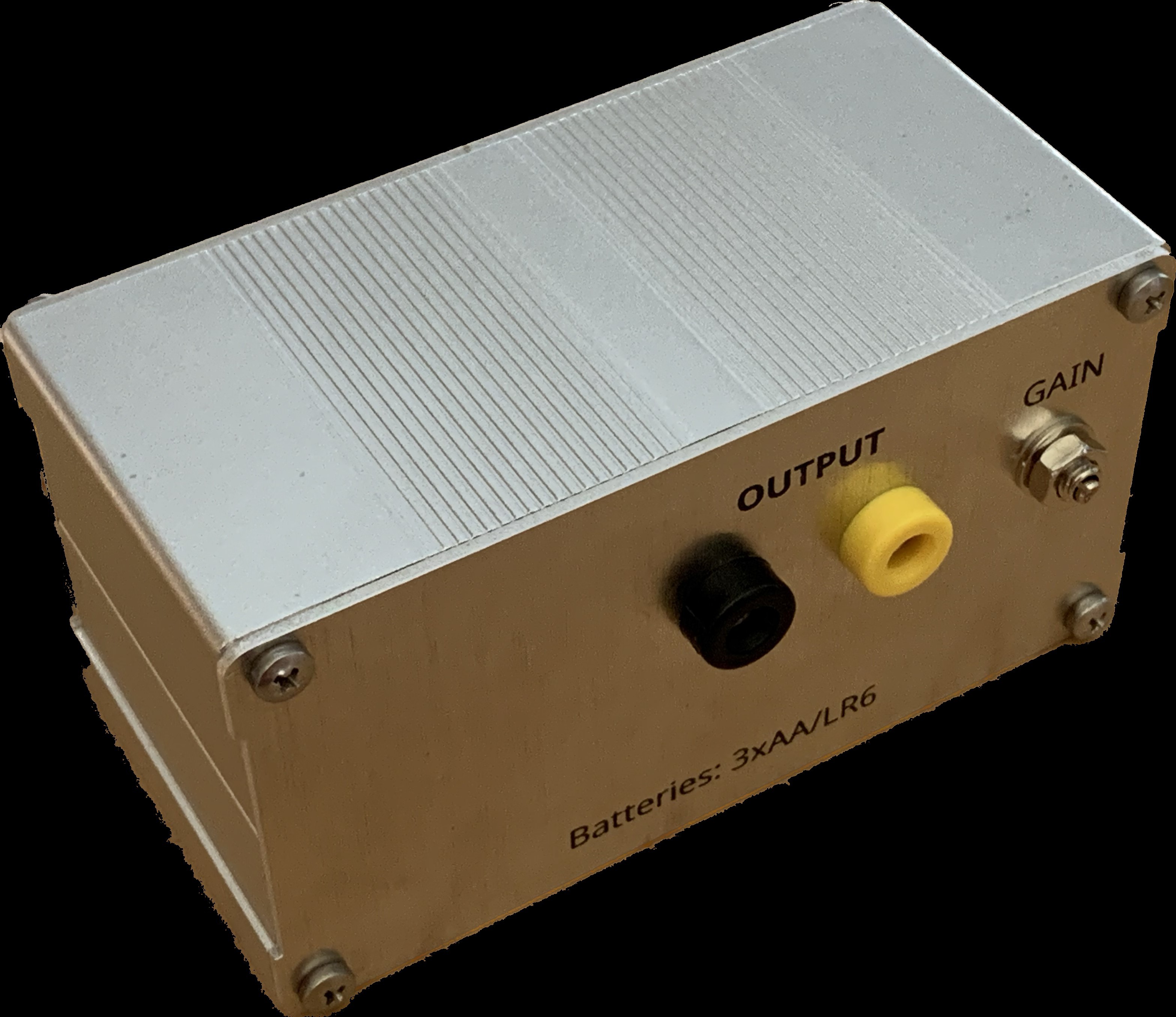
On the back, there is a 1V/Ω analog output, as well as the scale (gain) adjustment trimmer.
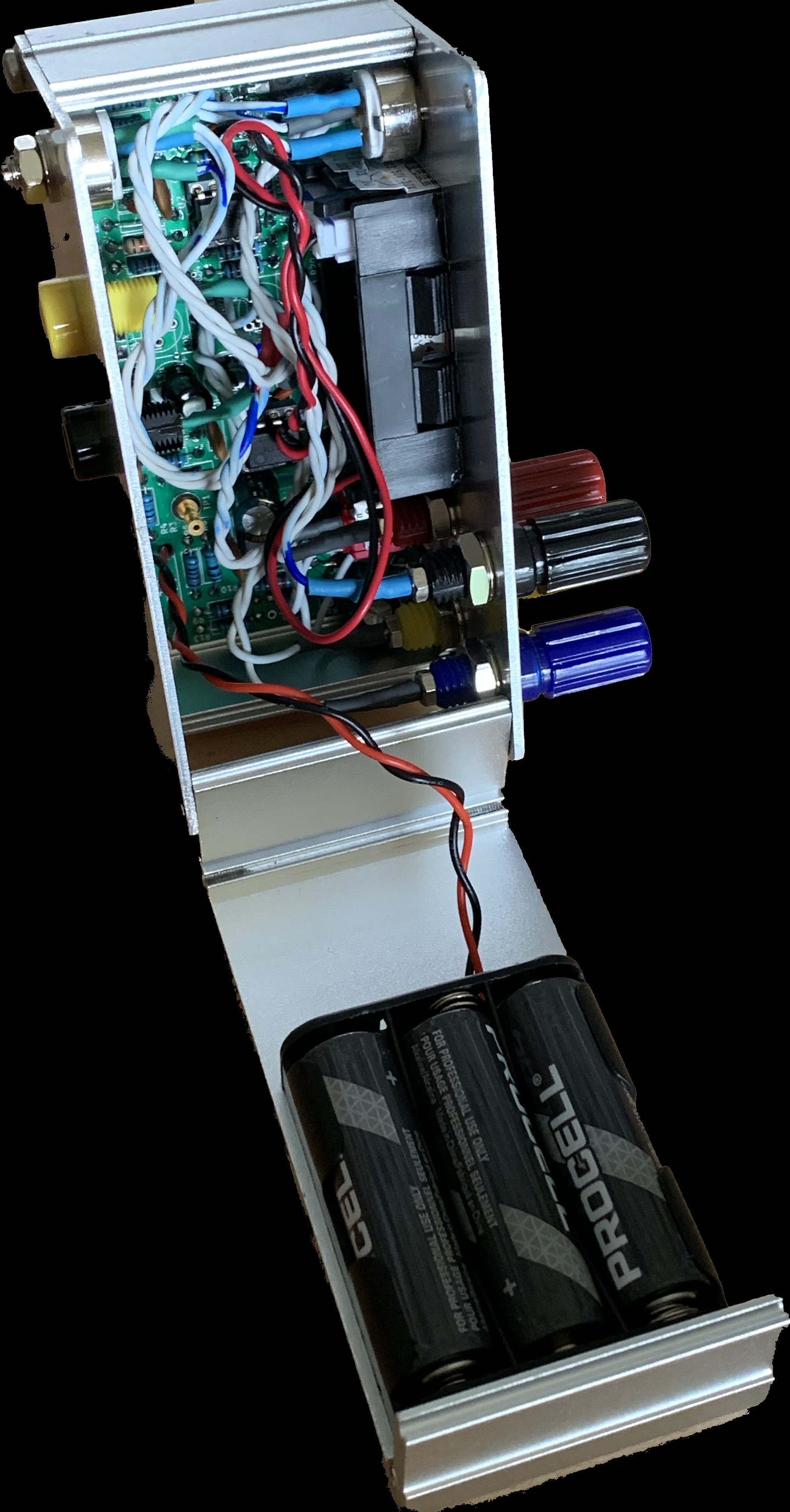
Access to the batteries is possibly by removing the 4 screws that attach the bottom half of the enclosure to the front and back panels, and swinging the bottom enclosure out.
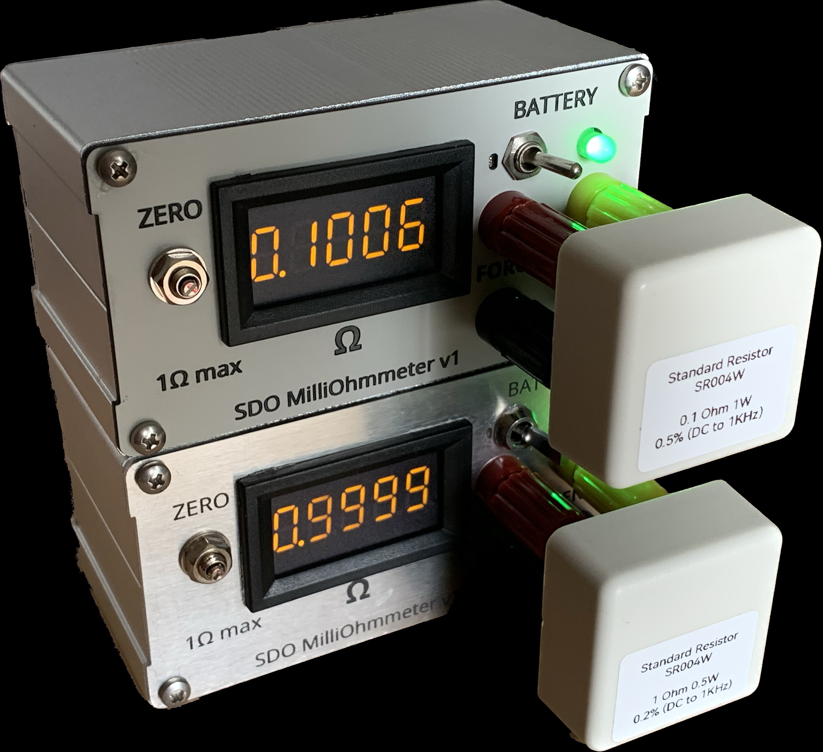
Two "clean" v1 rev1 prototypes were built - one with an aluminum front- and back-panel (bottom), and another with an acrylic front- and back-panel (top). The aluminum panels are much sturdier than the plastic ones.
For aesthetic reasons, the plastic "hp gray" front panel could be glued on top of a legend-free steel or aluminum backing plate to make the panel durable.
Overview of the Circuit
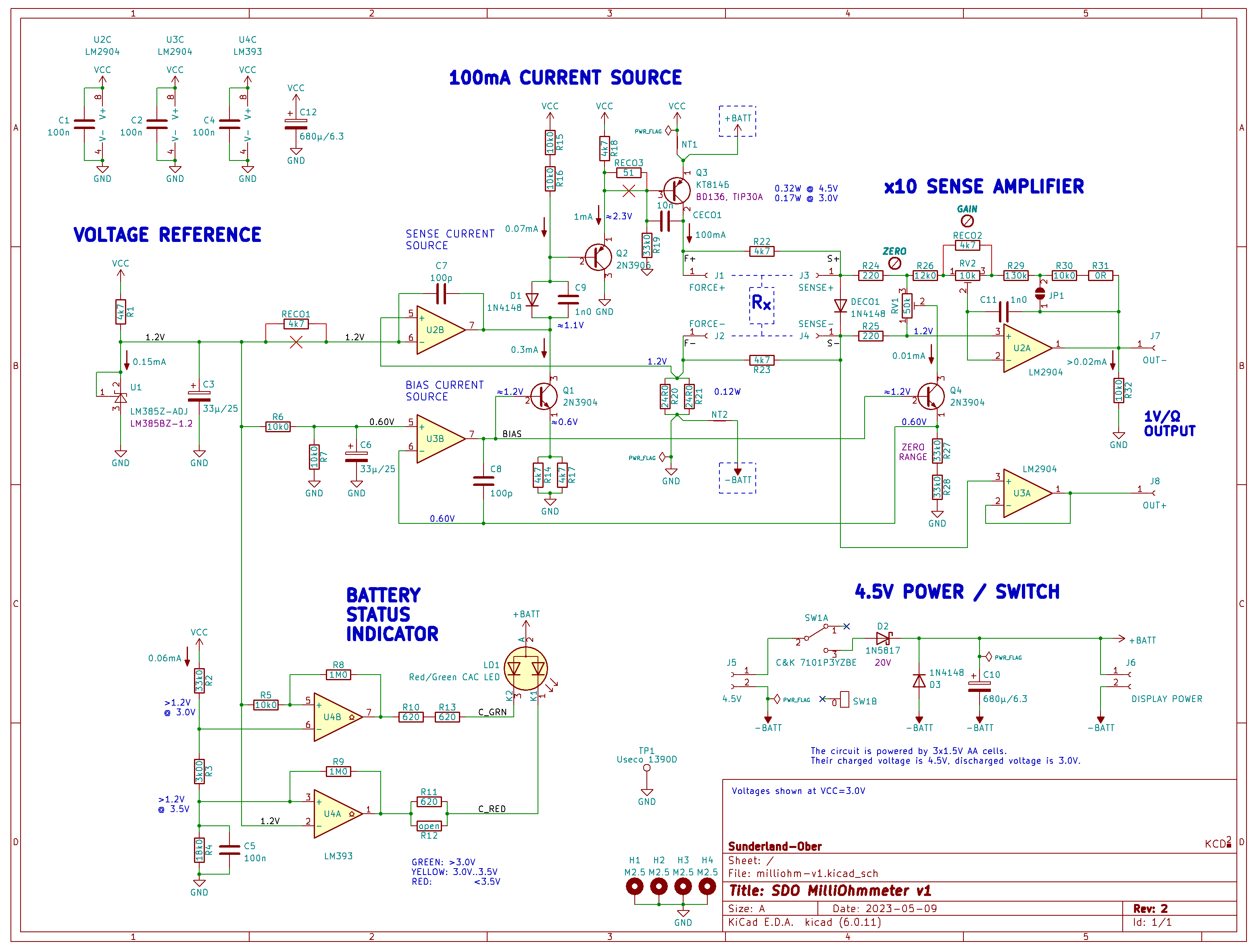
The circuit blocks are:
- 3xAA cells as a power source,
- 1.2V voltage reference (LM385),
- 100mA current source, using a 12Ω current sense resistor,
- a bias current source using LM358,
- a 10x inverting sense amplifier (LM358), driving the (-) output terminal,
- a voltage follower (LM358), driving the (+) output terminal,
- gain (full-scale) and zero adjustments,
- comparators (LM393) that monitor the supply voltage against 3.0V and 3.5V threshold, with a bicolor LED indicator,
- a 4.5-digit off-the-shelf panel-mount voltmeter as a display; an external voltmeter can also be used.
No differential nor instrumentation amplifiers are used, and resistors used are standard 1% types. The zero and full-scale (gain) adjustments are available externally.
I went for something that could be assembled from parts available in mid-to-late 1970s: "jellybean" general purpose op-amps and comparators, and mostly basic passive and discrete components. Most everyone who did electronics for a while will have compatible parts in their "junk" drawer somewhere. All the parts are also available on eBay. A 3.5-digit "jellybean" ICL A/D chip could have been used in the 70s in place of the modern 4.5-digit display.
Component Selection
The supply is 3 alkaline AA cells in a de-facto standard plastic battery holder installed on the bottom half of the enclosure. An optional external power supply could be, for example, Nokia ACP-7U 3.7V "brick" rescued from e-waste.
The basic requirement for both op-amps and comparators used are simple:
- Specified for operation from 3V up to at least 5V (can be higher of course),
- Input (common mode) voltage range down to V-,
- Output voltage range down to 0.2V at low currents,
- Input and output voltage range up to V+-1.5V.
The ubiquitous and cheap LM358/LM2904 dual op-amp and LM393/LM2903 dual comparator fulfill these requirements and work fine in this design. TL072/082 won't work, since they need a higher supply voltage, and their input range includes V+, not V- as needed in this design. The use of a comparator is required - LM358 won't work due to its inability to pull the output pin down close to ground while sinking several mA from the LEDs.
The small-signal NPN and PNP transistors in TO-92 packages can be any general purpose type and are not critical. High beta is not required. 2N2222, 2N3904, BC547 and their PNP complements all work well.
The medium-power PNP transistor also can be any silicon type with ft>2MHz, although the pinout used is ECB since that's the transistor I found first in my junk box. A TO-92-packaged part could be used as well. It will just run warm/hot to touch. I opted for the TO-126 just to keep it cool.
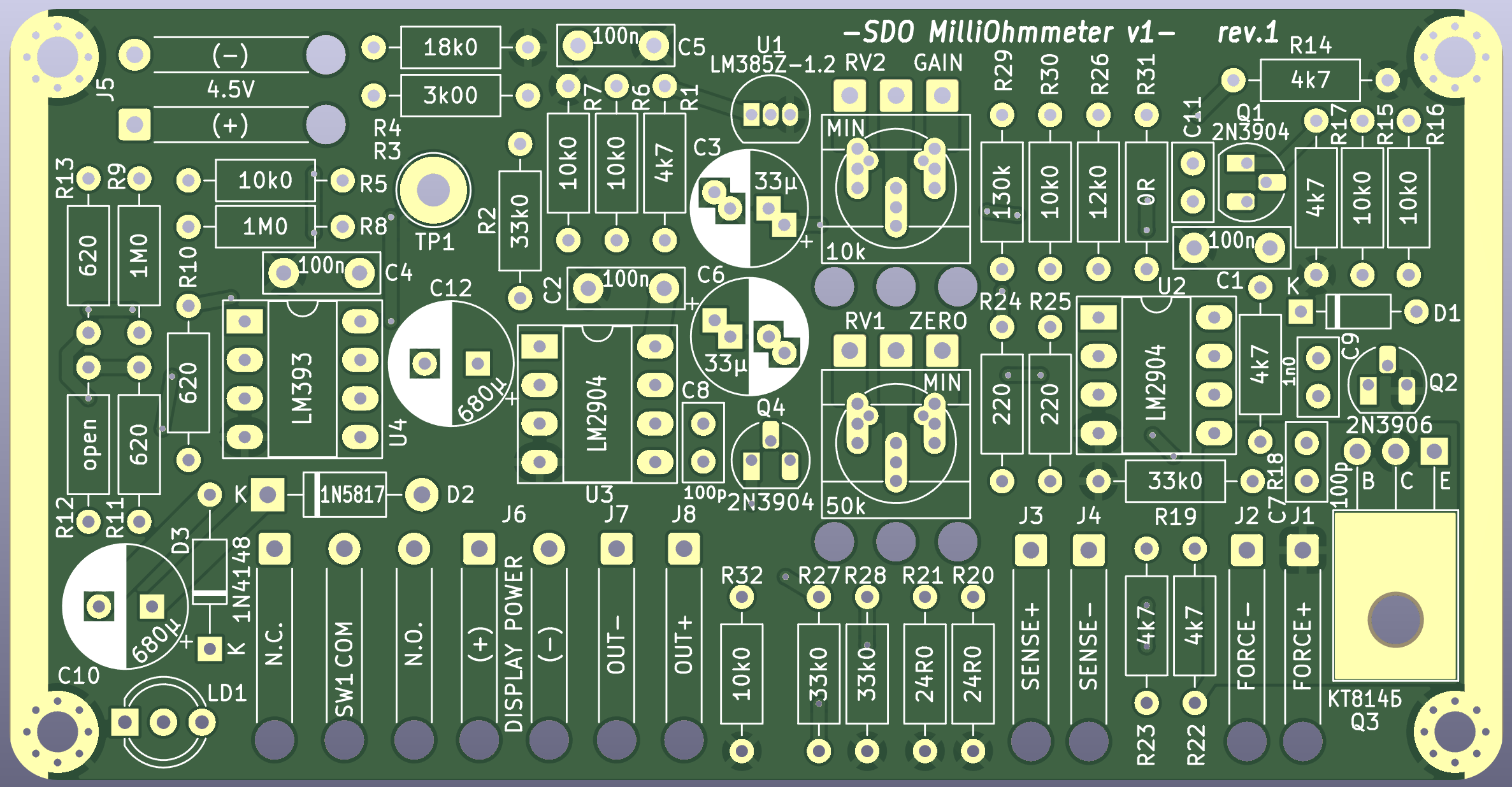
Board Layout
The PCB's top layer is a mostly continuous solid ground plane. The signal traces are on the bottom layer. The connection points for the wires are provided with stress reliefs. The potentiometer footprints are custom and accommodate several common potentiometer styles, as well as a wired off-board connection.
The silkscreen has the part values marked for ease of assembly. Of course, for an initial prototype, a few of the values have changed, and there were a couple extra parts installed on the board. These parts have the xECOx reference designators on the schematic.
Detailed Narrative
Power Input and Distribution
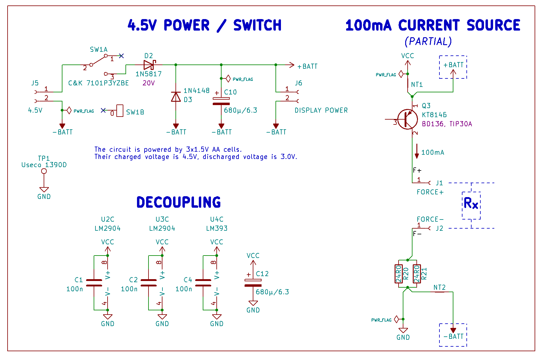
Fig.1. The power input and distribution circuit.
Power Input: A 3xAA battery holder is connected to J5. The battery voltage is 4.5V with fresh batteries, and 3.0V when the batteries are fully discharged. The front-panel power switch is SW1. The input is protected against reverse voltage by the series Schottky diode D2. This diode can have up to 1mA of leakage when reverse-biased. This leakage is shunted by D3, assuring that the rest of the circuit doesn't carry from negative supply currents.
Power Routing: The top of the PCB is a ground plane, connected to battery (-) at the bottom end of the current sense resistors R20||R21. The VCC rail, between 3V and 4.5V, is connected to the battery (+) at the collector of the 100mA source transistor Q3. This ensures that the 100mA force current does not flow through the ground plane nor through the VCC polygon on the bottom layer of the board.
Decoupling: The op-amps U2, U3 and the comparator U4 have their supply pins decoupled with 100nF. A 680uF bulk capacitor is connected to the battery side of the supply, as well as to the VCC side of the supply.
Test Point: TP1 is a handy turret test point connected to ground. It's useful when troubleshooting.
Voltage Reference and Battery Voltage Indicator
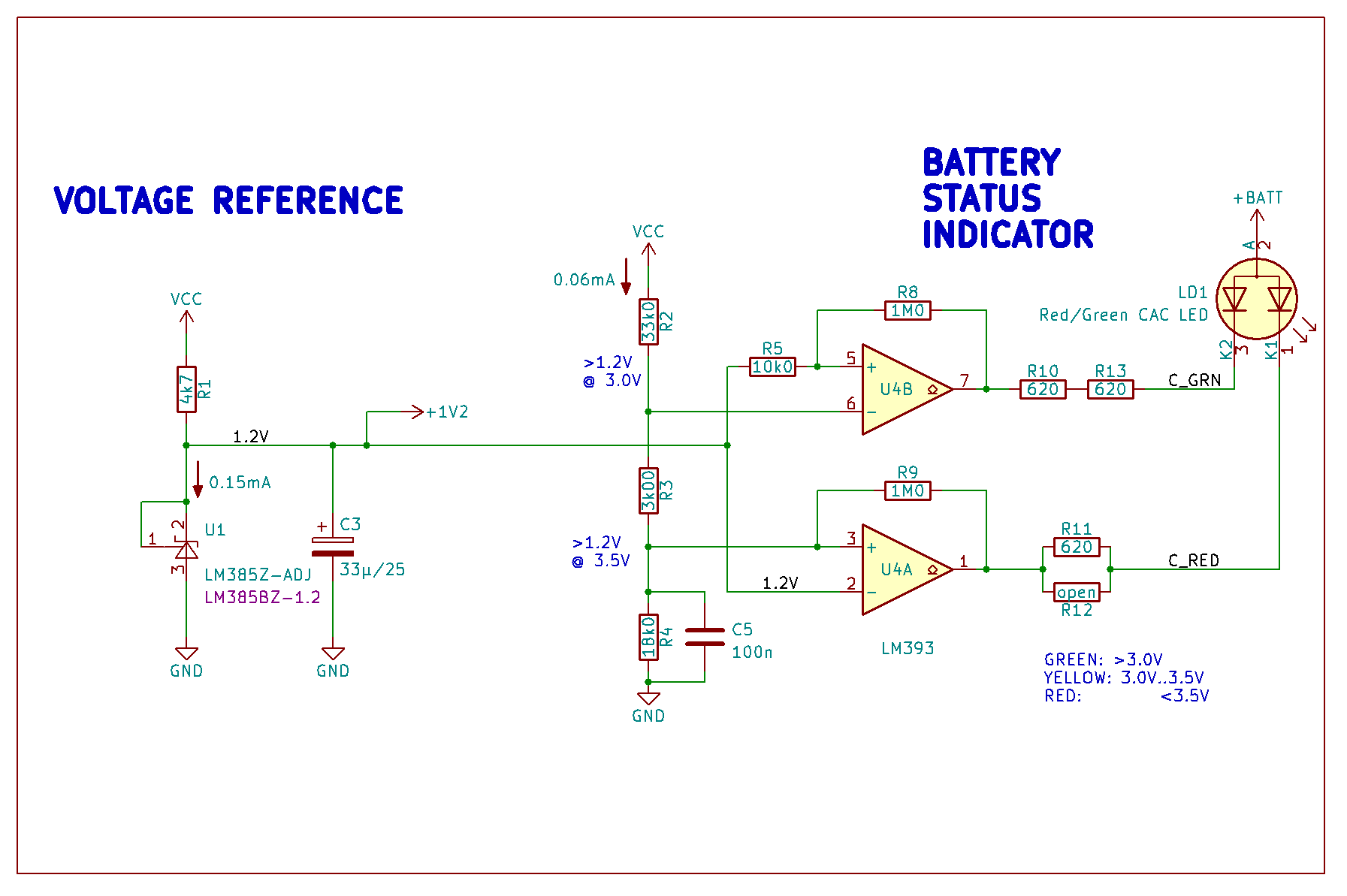
Fig.2. The voltage reference and battery status indicator circuits.
Voltage Reference: R1-U1-C3 generate a 1.2V reference voltage for the rest of the circuit.
Battery Status Indicator: A bi-color red/green LED LD1 indicates the supply voltage status. It is green above 3.5V, yellow between 3.0V and 3.5V, and red below 3.0V (the minimum operating voltage for the circuit). When the supply voltage is too low, the measurement results are no longer valid.
Battery Status Comparator: The double comparator U4 (LM393/LM2903) is configured to light the red led below 3.5V, and the green led above 3.0V. Between 3.0V and 3.5V, both colors are on and mix into yellow. R8 and R9 provide hysteresis necessary to prevent oscillations close to the threshold voltage. The divider R2-R3-R4 scales the battery voltage to 1.2V at 3.0V and 3.5V for U4B and U4A respectively.
Force Current Source
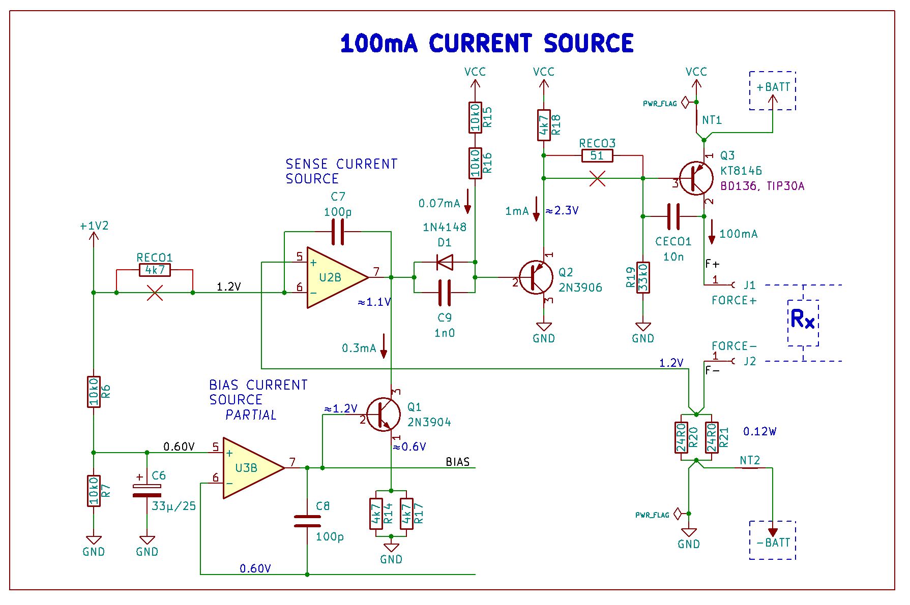
Fig.3. The force current source and the partial bias circuit.
Ohmmeter circuit: The resistance-under-test Rx has a 100mA current driven across it. The voltage dropped across it has a 0.1V/Ω scale factor. It is amplified 10x to provide the 1V/Ω output to the display and external output.
The bottom of Rx has a fixed potential of 1.2V. The top of Rx is at 1.3V at full scale of 1Ω, and at 1.2V at zero Ω.
100mA Force Source: The reference voltage is duplicated on the current sense resistor R20||R21 by the current control loop. U2B closes the loop around the source Q3 and the current sense resistor R20||R21. The drift of the latter has primary impact on the stability of the measurement current.
Q3 is a common emitter stage and adds voltage gain at low frequencies to the op-amp's feedback loop, when compared to an emitter follower more typically used in such circuits. This improves the current regulation accuracy.
Q1 loads U2B's output with approximately 0.3mA of sink current, forcing U2B output stage to operate in class A. This improves the transient performance of the relatively slow LM358 and improves stability by lowering the output impedance slightly.
D1 and Q2 shift U2B's output voltage range up to Q3's base potential. U2B's output range is from V+-1.5V down to V- and is too low to to directly control Q3's base.
Bias Current Source: The 1.2V reference voltage is divided down to 0.6V and filtered through R6, R7, C6. The bias current source regulator U3B provides a Vbe-tempco-compensated offset copy of the 0.6V reference. This biases Q1 for approximately 0.6V on the emitter, and sinks 0.3mA from U2B's output, biasing it into class A operation.
Modifications to Rev 1 PCB Layout:
- RECO1 was added to allow U2B to be compensated,
- RECO3 was added in series with Q3's base to limit the base current when Rx is not connected,
- CECO1 provides phase lead at higher frequencies, stabilizing U2B
Sense Amplifier
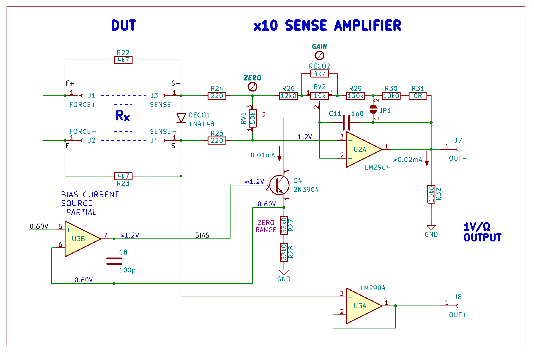
Fig.4. The sense amplifier circuit.
(-) Sense Amplifier: U2A is an inverting 10x amplifier. The input and output voltages are not referenced to ground, but to the approximately 1.2V potential at the bottom of Rx. This is of no consequence since the digital voltmeter as well as any external voltmeter have differential inputs. The 1.2V difference between the battery ground and the output "ground" is only visible inside of the ohmmeter.
The sense amplifier output voltage is 1.2V when Rx is 0Ω, and 0.2V when Rx is 1Ω. The sense amplifier provides the variable negative (-) side of the output voltage!
JP1 is provided for diagnostic/bring-up purposes only.
Output (+) Follower: U3A buffers the negative sense terminal, nominally at 1.2V. The follower outputs the relatively constant 1.2V (+) side of the output voltage!
This approach keeps the sense op-amps at a constant common mode voltage. This reduces the impact of the relatively low CMRR of jellybean op-amps used.
There's also no need for tightly matched resistor networks as would be required in a fully differential amplifier, e.g. as used in the inspiring project.
Open-Circuit Detection: R22 and R23 couple the sense inputs to the force outputs. When Rx is absent, this saturates the sense amplifier output at least 50% above full scale (>1.5Ω readout). This is the indication to the user that the input is "over-range".
Offset Nulling: The input offset of the U2A sense amplifier is nulled by adding a voltage in series with the input. Resistors R24 and R25 generate the differential offset null input voltage by sharing a 10µA load current, apportioned between them via RV1 zero adjustment potentiometer.
Q4, R27+R28 and U3B take the reference voltage and use it to provide a stable 10µA load current for offset nulling.
Modifications to Rev 1 PCB Layout:
- RECO2 was reduce the gain adjustment range to make it easier to dial-in the gain,
- DECO1 was added to limit the sense amplifier input voltage to about 0.6V. This allows the sense amplifier to provide reliable "overrange" output when Rx is open or more than 1.2V.
Possible Improvements
Short-term Drift
Almost all of the short-term output drift comes from the sense current drift. This drift is caused by the heating of the current sense resistors. Those are the parallel pair of 24Ω, 1/4W resistors R20, R21. These resistors cycle between 60mW dissipation each when the load is connected, and 0mW when the load is disconnected. That's why it takes a dozen seconds or so for the last digit to stabilize enough to be useful when using 1/4W parts as suggested by the PCB layout.
I have used "eBay deal" resistors that seem to be low quality - very thin terminals and high tempco, at least 100ppm/°K or more. Those of you without stock of quality resistors are likely to run into the same problem.
Workarounds
- Use lower tempco resistors for R20||R21. This trades off short term drift for more specialized parts and slightly higher cost. I've replaced R20, R21 with a 2W 12Ω 20ppm/°C resistor and it solves the short-term drift problem. It's the only less-than-usual part needed in this design. or
- Connect a silicon diode from the Force+ to Force- terminals, causing the 100mA current to flow continuously. This brings the sense resistor into thermal equilibrium, but trades off short term drift for battery drain. It's less of a concern when using a mains supply.
Temperature Drift
Remainder of the offset drift comes mostly from the op-amps, and in small part from the offset null network. Choosing lower-tempco op-amps takes care of majority of this temperature-induced drift.
Power Dissipation
The sense current is sourced using a linear (non-switching) source. About 0.45W of power is dissipated by the force current flow at high battery voltage, down to 0.3W when the battery is fully discharged. Very little of this dissipation occurs on the device under test - 0.1W across a 1Ω resistor, down to 0W across a 0Ω resistor. This is a tradeoff needed to keep the circuit simplest.
A switching buck converter could be used to provide a high-efficiency 100mA current source. Alternatively, the current could be pulsed, and a low-drift analog sample-and-hold could be used to hold the sense voltage between the samples.
Non-Ratiometric Operation
The digital display module has an A/D converter with internal voltage reference, without provisions for external reference input nor for internal reference output. This introduces a requirement for the ohmmeter voltage reference to be stable versus the A/D internal voltage reference.
A custom display circuit could circumvent that problem by using the same voltage reference for both the A/D converter and the measurement current source.
Positives
The gain (full scale) is quite stable since it's determined by a resistor ratio that is relatively insensitive to temperature changes. The voltage reference has no appreciable impact on the full-scale drift.
The voltage gain of the sense amplifier is only 10x, thus the op-amp offset drift performance is not very critical. LM358 is good enough.
The offset null network is stabilized against Q4 Vbe drift, and has first-order compensation against tempco. As R27+R28 resistance increases, the offset nulling current flowing through Q4 drops, lowering the voltage drop across R24/R25. This is compensated by the R24/R25's values also increasing, increasing the offset null voltage, and thus mitigating the drop in the offset null current.