Gathering components.
The TCD1304AP has a good sensitivity in the wavelength range of 400 - 700nm, allowing to apply a 650nm laser. Such diode lasers are widely available and very cheap, I apply a Chinese one of less than €5.-. The prism comes from Hong Kong for just below €19.-, while I bought 2 CCD-chip’s in China for less than €23.- And 2 Blackpill MCU boards (STM32F401CCU) were ordered for less than €9.-, also in China.
First steps.
At first I tried to bypass the nasty details of the readout of the CCD-chip by ordering a small board with a programmed MCU. It should drive the CCD and deliver the data in bytes over its serial TTL output, followed by a small TTL to USB converter. The boards arrived, already connected by a short 4 wire Dupont cable, without any documentation or instruction (usual with AliExpress. I connected the USB-C and tried to collect the expected bytes. No success. After a short time I discovered the CCD chip and the voltage regulator on the MCU board were really hot. Further inspection learned there was a connection error: the pre-connected cable was swapping the V+ and Gnd, baking the various semiconductors. After some struggle and intervention of AliExpress, I got a full refund of the paid €34.37!
This adventure learned me to go the hard way: learn how to program the MCU myself. In the meantime I had read stories of other technical enthusiasts, and understood that the coding of STM MCU’s is a big difference from programming an Arduino. So I bought myself a Nucleo-476RE board and started to follow a lot of tutorials, introductions and other information to master the Nucleo board with the STM32CUBEIDE. I considered myself lucky to have gathered some experience with Arduino’s and followed an online C++ course, it helped me to understand the new stuff more easily.
However, in the beginning I got mad with all acronyms: as newbie in this area of programming, it is like hearing old Greek or Chinese, no idea what is meant. I made myself a list with all new abbreviations plus their meaning, that helped me learning. I also read regularly advises to skip the ‘bloatware’ of the STM IDE and program the registers directly, because that’s where after all the actions are defined. I considered that approach too difficult for me, in that stage I only had a vague idea of how registers control the actions of the MCU.
Getting started.
Via the Hackaday site I found some other guys who are/were working with TCD1304 CCD’s. The extensive explanation of ‘Curious Scientist’ of building an application for the readout of the photo-diode signals appeared also a hands-on introduction of the STMCUBEIDE, I learned a lot from him. Another guy, Esben Rossel, proved to be very interested and helpful, although he worked with such CCD years ago. He also sold me a small PCB with some SMD components mounted like proposed in the Toshiba Datasheet, so I didn’t have to make it myself.
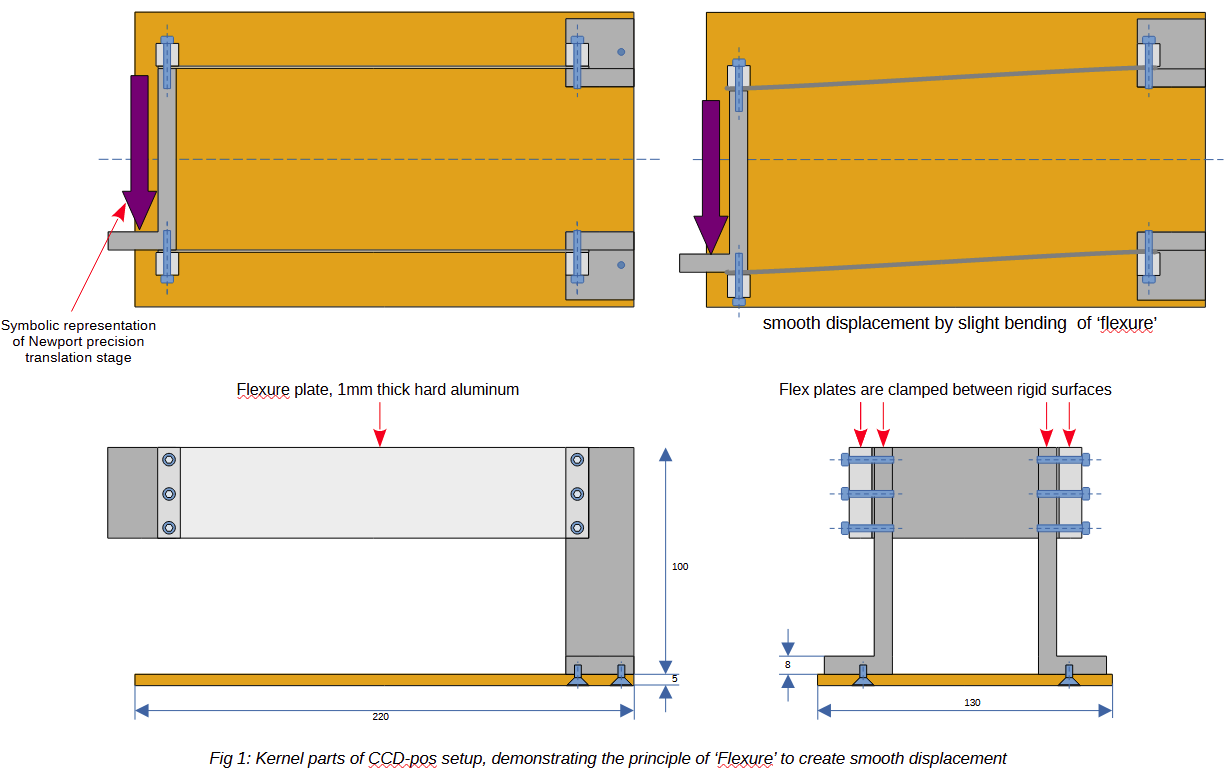 The mechanics were completed with the mounting bracket for a 5mW 650nm diode laser, including a simple but effective adjustment mechanism. The prism is glued with double sided tape to a small Aluminum strip with slits, bolted to a L profile to allow perpendicular positioning against the laser beam. The L profile has vertical slits to make horizontal alignment possible. The CCD PCB (bought from Esben Rossel) is bolted to a small poly-carbonate rectangle with an opening to let the CCD-chip through, a second slit for the 6pin connector and four threaded holes for mounting. The main rectangle and the PCB got an additional nock to let the laser beam pass by as close as possible to the short side of the CCD chip. This is required to apply the maximum of the width of the prism for reflection and use the full range of pixels. The sketch in fig2 shows these items and in combination with the sketch in the description illustrates the principles.
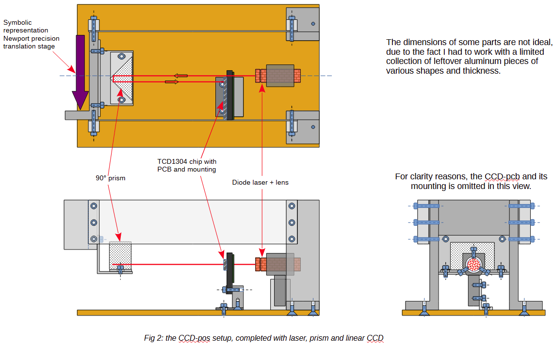
The depicted layout is the result of quite a long development period, where a number of things were improved, changed, rearranged, etc. to end up with a layout that is easier to handle and align. Especially alignment proved to be a nasty issue, which is inevitable when one tries to work in the (sub-)micron region.
Another issue was the laser: I bought several types of very cheap laser modules (> 1 Euro a piece) and some a bit more expensive (~4 Euro) from AliExpress. All modules gave a reasonable beam that even could be focused a bit, but the beam direction of the really cheap ones showed quite an angle wrt. the housing and so the lens. Changing the spot size meant a considerable spot move, which drove me mad while tuning. The 4 Euro one was mechanically more robust, has a separate laser "chip" and even an interchangeable lens, so I selected that one for further development.
To improve the quality of the laser spot I created a collimator by gluing several small rings on top of each other, the smallest one with a round hole of ~1 mm. In a later state I intend to do more research on manipulation of a small laser beam, but for now I work with a collimator and single focus lens.
The Hitachi TCD1304 appears to be very sensitive for ambient light, which can obscure a considerable to even major part of the laser spot. To prevent this effect, I created a simple shielding from the metal of a scrap cigar can. After soldering the parts together I sprayed it with mat black paint to reduce reflections. This appears to be very effective, reducing the 'dark voltage' to a minimum.
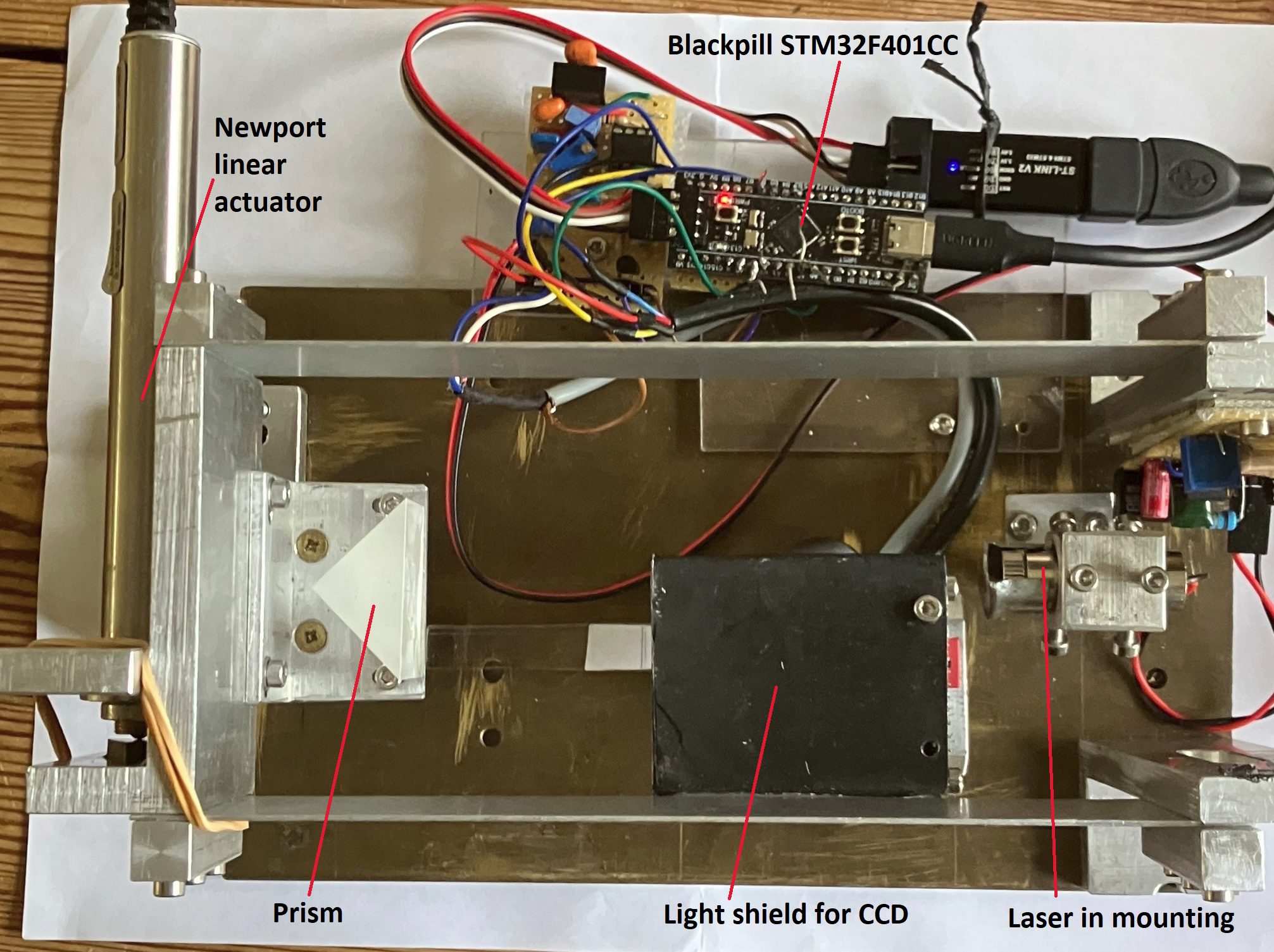 Fig 3: topview of the experimental CCDpos setup.
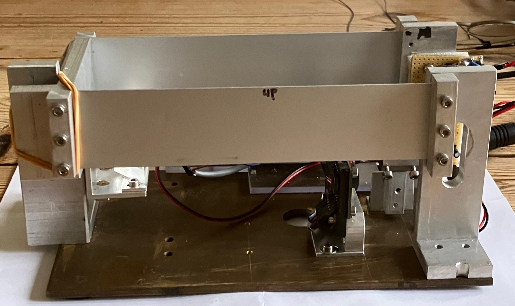
Fig 4: sideview of the CCDpos setup, showing the 'flexes'.
Simulation Ray-tracing CCDpos setup.
I wanted to show myself how the laser beam propagates through a system like CCDpos, to get some feeling for the influence of the angle on the position of the returned light. So, I created a simulation based on the physical laws for breaking and reflection of light on surfaces. The figures below show the path of the beam in two start conditions.
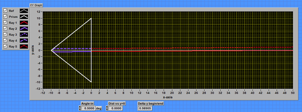
Fig 5: Ray-trace starting at y=0.0 with an angle of 0.50degree, resulting in a shift of 0.98905mm.
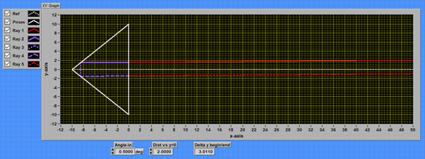 Fig 6: Ray-trace starting at y=2.0 with an angle of 0.50degree, resulting in delta-pos of 3.0110mm.
To quantify the influence of the beam angle at start I ran a set of simulations at a list of angles, the results are shown in the figure below: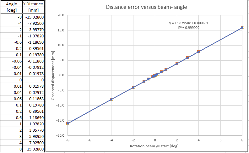
To my surprise the measured relation appears to be (almost 100%) linear, and substantial: 1.9867mm per degree!
This makes very clear the stability of the laser and its mounting must be extremely good when the aim is to measure displacement with nanometer precision.
Readout of the TCD1304 chip.
As the components on the CCD-board I bought from Esben Rossel only are inverting drivers and a transistor for buffering the signal, all needed signals must be delivered externally. I already learnt a STM32F401CC micro has all all required features to extract the light level signals and even digitize them. However, at first I applied my Nucleo-L476 board and connected the relevant pins to the CCD pcb, because my examples used that processor.
I started climbing the learning curve with careful following the steps that 'Curious Scientist' describes in (https://curiousscientist.tech/blog/tcd1304-linear-ccd-driving-the-ccd) . He has also made a YouTube video on the same subject. This guidance has got me going, after a while I could see a pulse of the laser beam on a scope channel!
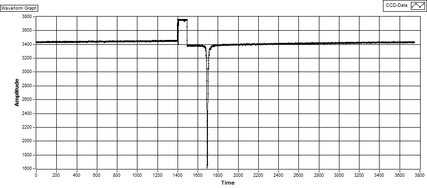 Fig 8: graph of an early set of data from the TCD1304; the high block @1400 .. 1500 is
the fake signal from dummy pixels.
Because I am historically very used to the LabVIEW programming environment and still have the ability to run it on my home PC, I created LabVIEW programs to collect and represent the CCD readout. Beside finding which bytes "belong to each other", there was another, more difficult issue. The MCU spits out a stream of bytes without any indication of their relation with the pixel position in the CCD. When put in a graph, the result was a peak, moving fast or slow to the left or the right. This was caused by a mis-match of the frequency of production and plotting, a kind of stroboscopic effect. Although I spent a long time to solve this issue, carefully reading the TCD1304 datasheet, a Toshiba application note, experimenting with different approaches, I never found a convenient and precise solution. I tried to mark the first elements of the data-array to be exported with a pre-defined code, that I could detect in the received data by the LabVIEW program. From these experiments I learned the DMA handling inside the MCU makes a simple synchronization by assigned marker values impossible. I managed to detect conditions for a steady (not moving)pulse, but these settings were empirical and needed re-adjustment after almost any modification. The need for a better solution remained, certainly because the final application is based on the precise position of the CCD pulse.
I already had seen a suggestion to improve the analogue signal from the CCD chip before sending to the ADC: the CCD produces an inverted signal with a certain offset from the max. amplitude, plus the pulse doesn't come even near the 0V level, because the pixels saturate before reaching such amplitude. An inverting opamp with offset compensation can solve these problems: the signal polarity can be "normalized", the amplitude can be increased to match the 0 ... 3.3V input range of the ADC and the offset can be reduced to get a maximal signal.
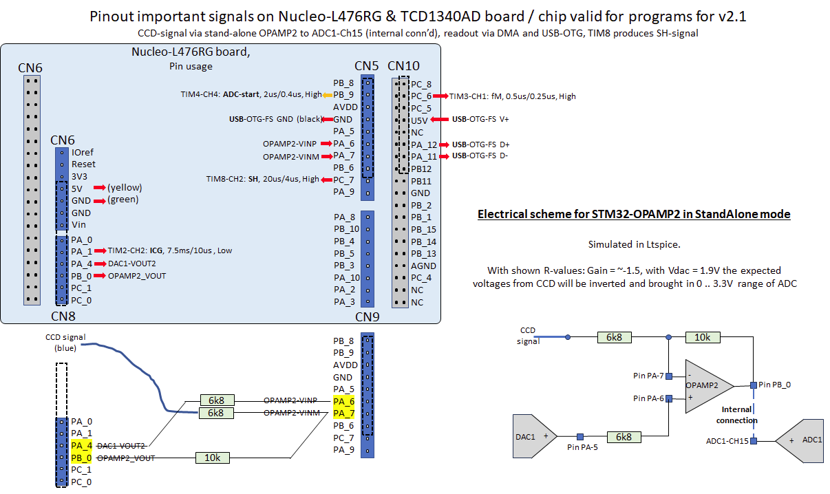 Fig 9: schematic overview connections Nucleo-476RE board
Another step towards the final design: a Marker.
Because the identification of the position of the CCD pulse remained a nasty problem, I decided to switch to another, more principle strategy. I want to inject a Marker pulse in the analog signal from the CCD, because such event can be reproducible synchronized with the readout sequence. Such injection can be done by adding a MOSFET that pulls down the CCD signal for a very short period just before the start of the readout of the pixels. Because such an extension requires more electronics, I decided to combine this modification with the switch from the Nucleo board to the We-Act v3 Blackpill board.
Implementation of Timers.
Once I felt more confident in programming timers in a MCU, I designed my own setup to fulfill the specifications for the TCD1304 signals plus my own addition of a Marker. As usual, the described layout is the result of a series of steps, additions, modifications, changes, retries, etc. The Blackpill board has some limitations in the export of signals, forcing me to be creative. Looking back, I am quite satisfied with the current design. It produces the signals for the CCD-chip, the ADC-trigger and the MOSFET for the Marker in a flexible way, allowing to tune delays where needed.
Although the requirements for driving a TCD1304 are already described in the datasheet and by others, I give here a short overview for completeness: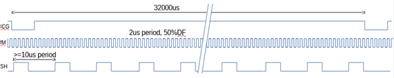
The essentials of the implementation are shown in the next figure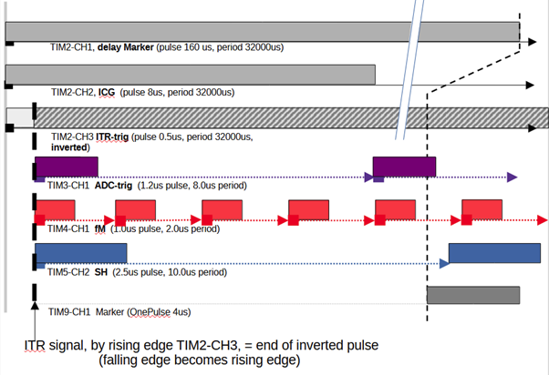
The base timer is TIM2, which produces three pulses with different functions:
- TIM2-CH1 is the delay for TIM9-CH1, which produces the Marker pulse,
- TIM2-CH2 produces the ICG pulse for the CCD,
- TIM2-CH3 is the delay for ITR mechanism to synchronize TIM3, TIM4 and TIM5 at every ICG pulse by a reset of the counters.
TIM3-CH1 is used to trigger ADC1-IN4 to digitize a new signal from the CCD (after conversion by the opamp PCB).
TIM4-CH1 produces the fM pulses for the CCD (the main clock for shifting the charges).
TIM5-CH2 produces the SH pulses for the CCD, which functions as an electronic shutter.
TIM9-CH1 is configured as ‘One-Pulse’ timer, which is triggered by TIM1-CH1. That signal is connected to TIM9-TI2FP2 (physically CH2), which triggers the generation of the pulse on CH1. This pulse is used to "fire" the MOSFET to pull down the input of the opamp that inverts CCD signal (see fig
Each readout sequence inside the TCD1304 is started when the falling edge of the SH-signal coincides with an ICG pulse. The delay between this moment and the output of the signal from the first “pixel” is not described, but can be measured with a scope. I apply a value of 160us, to ensure the Marker is created before the first pixel arrives in the data-stream.
I learned from Hackaday member ‘Curious Scientist’ that STM32CUBE-IDE accepts simple expressions as input for settings of Timers. like 250-1. This makes code a bit better understandable: the wanted value is 250 and the system adds 1, so the user must apply a correction. I found out this expression can even be more complicated: on many places I insert expressions like ‘(7*8 + 4.5) * 84 -1’. This is an example, which may be used when one wants a value of 7 times the period of 8us, corrected with 4.5us, to be used with a timer that runs on a 84MHz clock on a system that adds 1 to the setting.
This notation gives a hint for the reasoning behind the setting and makes it easier to edit changes.
I also found out it is sometimes possible to tune the start of a signal by adjusting the setting. I did it with the ITR-trigger (TIM2-CH3): the ITR mechanism expects a rising edge, which is created after CCR counts because the TIM2-CH3 signal is inverted.
I use MS PowerPoint for several purposes, like documentation, a drawing tool for simple mechanics, but also as tool to create a sketch for the layout of my copper strip experiment PCB's. Such sketch serves as way to create the layout and as documentation when the board is created and 'bestucked'.
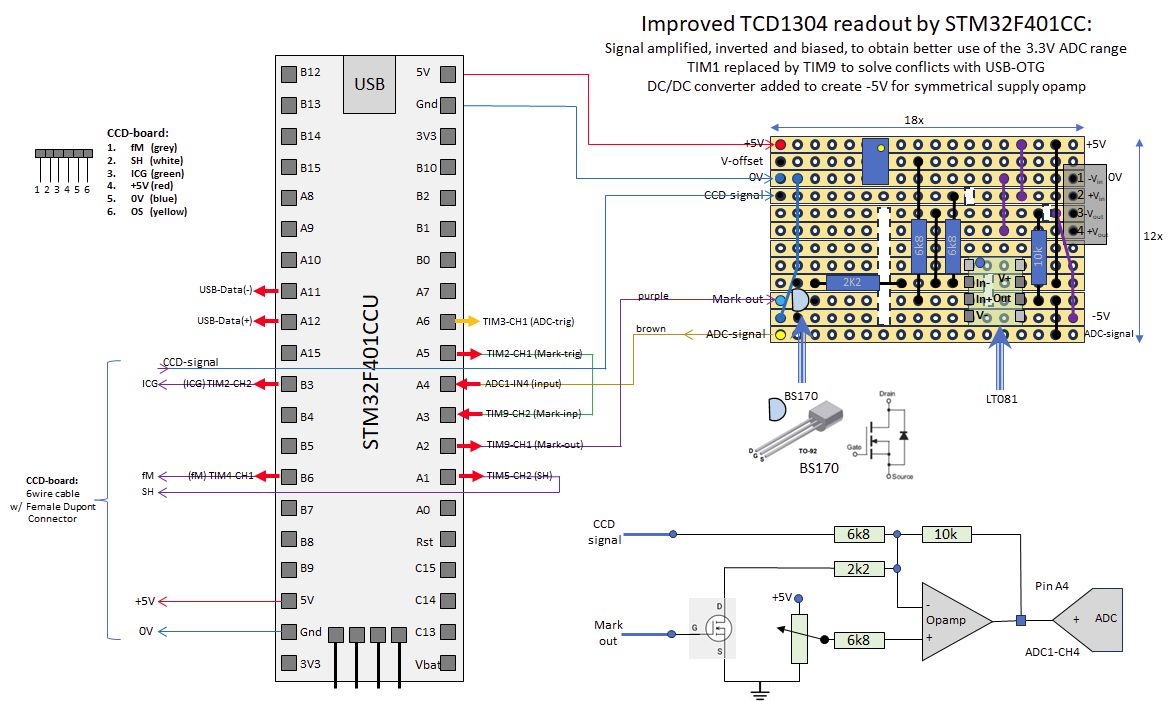 Fig 12: schematic overview STM32F401CC with separate amplifier, offset and Marker.
Readout with a Marker.
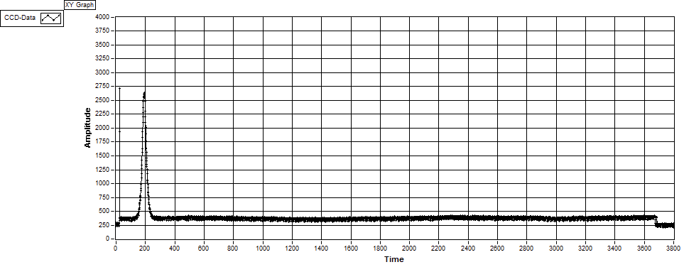 Fig 13: example of retrieved data: the narrow spike at the left is the Marker, the pulse near ch200 is the laser peak.
The next step is the determination of the exact position of pulse from the laser spot. In a first order approach such a peak has the shape of a Gauss curve. As start I use a peak finding function, based on the first derivative of the signal with some constraints. With this information a Gauss fit can be made, which delivers the center of the peak, resembling the center of the laser beam. At first sight this sequence seems to be sufficient, however reality appears more complicated. The bytes from the USB port arrive in chunks that may have sizes which differ from an entire readout, so it may be needed to search for a Marker-LaserPulse combination in separate retrieved sets of data. Plus in the original configuration the application runs at full speed (= the readout rate, allowed by the specifications of the TCD1304), so an output of more than 135 "frames" of >3648 pixels per second, or > 984kB per sec.
In such situations it is useful to apply a design based on the "Producer - Consumer" concept: two independent loops, one reads and stores the data (in the sequence of reception!), the other delivers chunks of stored data with a useful size, see fig .
Fig 9: schematic of Producer-Consumer concept.
This concept solves the problem of incomplete frames, as the next received bytes are seamless put after the end of the previous (possible incomplete) frame. However, it is not efficient to store almost 4k words while only 50 + 200 are needed to determine the Marker resp. the Laser peak. So I decided to make the Data-Storage more intelligent to detect the parts of incoming data to store, including some relevant parameters.
The intelligent Data-Storage.
In "Read Data" mode, the Data_Storage function receives chunks of bytes from the Virtual COM Port, with un-defined size (often 8000 bytes, but also more or less). The reconstruction to U16 words is simply done by casting the incoming array of bytes to an array of words, followed by swapping the bytes in each U16 word. Next, all elements of the U16 array are compared to be greater than a chosen value, mostly 1500 well above the baseline and lower than the peaks to be detected.
The search for the Marker is done in small sub-set of the boolean array, its length is 100 elements. At first this boolean array is searched for the first TRUE, probably the start of the Marker. When the index of the first TRUE is far enough from the end of the array (>= expected width of the Marker pulse), the next action is searching for the first FALSE, possibly the index of the end of the Marker. Otherwise a "new" sub-array is selected, 50 elements shifted, and searched for the first FALSE. The width of the pulse is calculated from the two indices and checked against a predefined lower and upper limit. When in range, the initial middle is calculated and the index and length of the set data-points to store. In case no Marker is found, the function determines to keep searching or abort the search and shifts a Frame-size elements to search for a following Marker. When a Marker is detected, the relevant values, including the data-array, are written to a dedicated structure, which is temporary kept apart.
The following action is to search for the Laser peak, which is performed by the same routine ('Find_Peak') with other values for a number of parameters, like 'search_length', 'min_' and 'max_width', 'length_to_store'. When 'Find_Peak' doesn't detect a peak with these parameters, the search array is shifted and the check repeated, until the whole "Frame" selection is done. In case a valid 'Laser-Peak' is found, the similar set of parameters plus a 'Data-array' is stored in an identical structure. When both a 'Marker' and a 'Laser-peak' are found in the same 'Frame', the 'Data-Storage' procedure store the two structures in its internal storage-arrays for Marker- and Laser-peak-data with an identical index. These arrays are circular with a defined size and a Write- and a Read-pointer to keep track of the position(s) to write to and to read from. The next figure shows how the LabVIEW code for this part looks: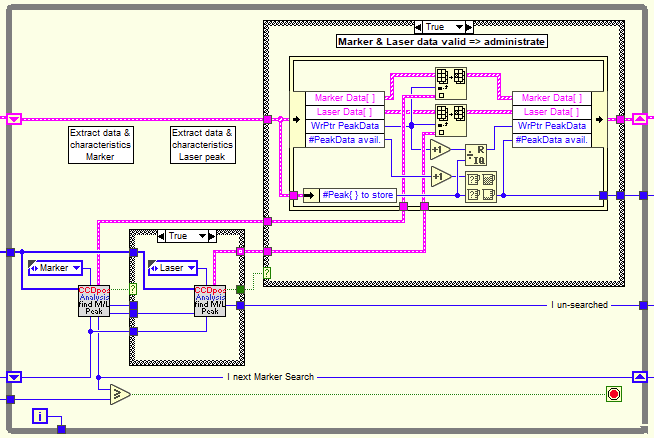
LabVIEW intermezzo.
LabVIEW is a graphical programming environment, where all primitives are represented by small icons. The arguments for input and output are connectors and the data "flows" through the "wires" from 'Indicators' (output arguments to 'Controls' (input arguments) of functions. The grey icons represent the 'Find-Peak' function mentioned before. The color and shape of the wires represent the datatype which "flows" through. The thick blue lines represent the incoming U16 data-array, that is delivered to both 'Find-Peak' functions. The white boxes with 'Marker' and 'Laser' are constant enums that specify the mode for each 'Find-Peak'. The thin dotted green line is a boolean value, which determines what code is executed when the grey rectangular boxes are "ready-to-run". These 'conditional' rectangles have 2 or more "layers", each with a possibly different content (empty is also possible). The value fed to the question mark connector determines which "layer" must be executed. The red-white dotted line represents the main storage structure of the 'Data-Storage' function. The white label-like blocks represent the extraction / assignment of structure elements, depending on the read/write mode (depicted with yellow on the left, resp. right side). The large dark-grey, rounded rectangle represents a while-loop, with a small square with 'i' as index and the red circle in a green square as continue/stop conditional. And again: all code inside the rectangle will execute after all incoming data is present, be executed as long as the conditional is not 'Stop' and "export" its data after it is stopped. Finally there are two 'shift registers' applied, comparable with a "static variable". They are shown as small rectangles per register, with a triangle inside, pointing down or up. The value fed to the right part is kept and is available at the left side when the loop makes a new iteration.
A base rule in LabVIEW is that any piece of code (a function, a primitive, a loop, etc.) cannot start execution before all incoming data is present and will not output any data before execution is finished. This means the sequence of execution is totally determined by how the pieces code are wired together.
The shown piece of LabVIEW code behaves as follows:
- when the while-loop is entered the current values in the main storage structure, the incoming Data-array, the index to start in the Data-array and the length of the Data-array is provided,
- all inputs of the left 'Find-Peak' function got their data so this function executes. The boolean output is TRUE when a valid peak is found,
- the shift register below contained the index to start searching, 'Find-Peak' delivers the new value to start searching in the next iteration of the while-loop, which is stored in the shift-register,
- when the first 'Find-Peak' had success (TRUE) the conditional right-next to it will execute the shown code, which means 'Find-Peak' in 'Laser' mode. When also a valid 'Laser-Peak' is detected, this conditional exports a boolean TRUE, an integer 'I_unsearched' and a structure with the relevant 'Peak-Data' of a laser-peak.
- the exported boolean TRUE sets the big conditional to execute the shown code, which means that both 'Peak-Data' structures are copied into the main storage structure and the administration is updated (Wr-Pointer, Nr-PeakData-avail.). Note that the index is treated specially because the main storage is a circular buffer and the number-avail. is limited to the length of the storage-array.
It is probably clear already, I am a supporter of LabVIEW. I use it since 1998, version 3 (distributed on a set of about 16 floppy disks), at this moment LabVIEW 2023 is actual. The package is very complete, has lots of useful tools and features, a wealth of >3000 'instrument drivers' (interfaces for all kind of devices) and a rich set of additional toolboxes for more specialistic applications (like 'Advanced Analysis', 'Spectral Analysis', 'Filter Design', 'Database Access', 'Vision', 'PID Control'. Based on the same drivers, there is also LabWindows/CVI, an ASCII based programming environment with many features from LabVIEW. Additional to this all there is also a huge collection of additional tools, collected in VIPM, the VI Package Manager, like LabVIEW and LabWindows, distributed by National Instruments.
National instruments features also a wide range of PXI chassis with and without embedded processors and FPGA's, focusing on reliable and fast Real-time applications.
Back to the CCDpos project.
Once the basics of the data handling are tackled, the main objective comes into view: how to determine precisely and reproducible the "distance" between the Marker and Laser-peak in fractions of pixels. With the aim of nm precision, the distance must be detected with 1/4000 pixel reliable precision: a pixel has 8um width, and the prism doubles the shift of the laser-beam, so 4um shift of the prism equals 1 pixel on the CCD.
At first sight, the detection of the Marker position looked to be very simple: the signal rises from background to almost full-scale in a one pixel step and returns to background the same way. One would say the middle between the first and last high pixel is the center of the Marker. However, although the Marker injection pulse is well-defined related to the other timer signals, the relation between the moment a pixel voltage is output by the CCD and the sampling by the ADC is not clear. Luckily, the mechanisms behind the appearance of the Marker and the Laser pulse in the output stream are "rock-solid" steady, meaning the relative position of the pulses only change when the Laser pulse hits another segment of the diode array in the sensor.
As mentioned before, the code in the 'Reading part' of the readout application does the initial scanning of the data stream, detects the presence of a Marker plus a Laser peak and stores the relevant data of the peaks plus some parameters for final analysis, see fig 10. This procedure prevents the storage of big amounts of data (~4000 words per Frame) with its processor load, while the code in the 'Consumer part' has the essential data to start with.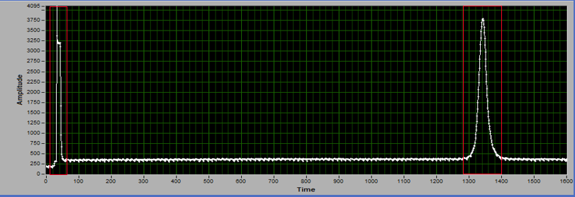
The code for precise determination of the middle of both peaks is quite similar, only the reference shape the algorithm uses to map precisely on each of the peaks differs. Next figure illustrates the two cases: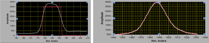
The principle for determination of the Middle position is based on making correlations of the measured data and the reference shape. LabVIEW supports a function that calculates the correlation of two inputs, resulting in a data array of double length. For better performance and easy interpretation of the resulting data, only subsets of the shown datapoints are used. The function calculates 7 correlations, where the measured data remains the same, but the reference data-set is shifted in X. The X-shift is -3, -2, -1, 0, 1, 2 and 3 steps along the X-axis. The resulting plots for the Marker are shown in Fig 13: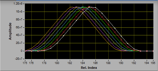
Of each correlation output array the middle part is selected (omitting the horizontal ends) to make a 2nd order polynomial fit, from which the Y of the maximum can be calculated. Next, these 7 Y-values are fitted against the related offsets (shift values) to find the X of the highest maximum.
The first time this procedure is performed on the measured points on the (integer) X-values, meaning a X-correction of 0.0. Now, the measured values are "shifted" the just determined X-correction by the LabVIEW function 'Interpolate'. This function takes the Y- and X-arrays of the (measured) datapoints as input and interpolates new Y-values for a third input array of new X-values. The previous described procedure (making 7 correlations and determination of the X-coordinate of the best -highest- correlation) is repeated on the new, shifted dataset to get another, more precise value for the middle of the Marker. This amplitude of this result (which may be the next X-shift) is checked to be less than the equivalent of the wanted measurement precision to determine if another cycle is required.
A similar version of the above described procedure is used to determine the precise middle of the Laser pulse. However, instead of a block shaped reference, here a calculated Gauss-curve is applied, constructed with the parameters of a Gauss-fit on the measured dataset. Tests revealed most of these parameters (amplitude, standard deviation and offset) hardly change during the shift cycles, so repeated Gauss-fits will only cost processor power without adding precision. The only changed parameter is the 'center' of the Gauss-curve, where the 7 shifts and the X-corrections are applied to.
Signal speed and sampling.
Now both the X-coordinates of the Marker and the Laser pulse are determined, the "absolute" position of the Laser pulse can be calculated in "index" units which equal to 'sample number'. The physical meaning depends on the specifications of the CCD-sensor and how the output of the sensor is processed.
The default mechanism for the TCD1304AP is described in the Toshiba datasheet and in a part of a Toshiba Application Note: three signals must be delivered to the CCD chip, being ICG (which clears the collected charges of all photo-diodes), fM (the data clock signal to shift the charges to the output amplifier) and SH (which determines the period to convert incoming light to electrical charge). Beside these signals three more wires are needed, one ground (combined, for power and signal), one for 5V power and finally a wire to guide the signal from the chip to the controlling electronics.
The typical frequency for the fM data-clock is 2MHz which results in an output rate of 0.5MS/s, in other words for each 4 fM cycles a data-value is available at the OS output pin.
The datasheet also specifies beside the 3648 "useful" signal elements a number of additional positions, 32 "before" the "useful" ones and 14 after them. It is not explicitly stated, but it looks like the system handles the 32 elements in front first, then the 3648 'main' elements, followed by the 14 at the end of the row and repeats this sequence permanently.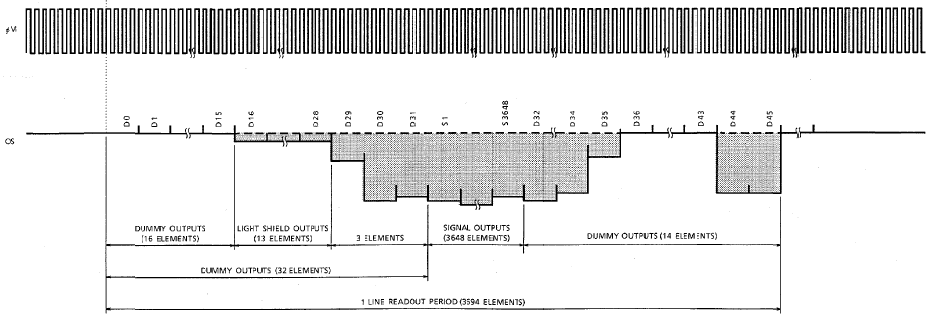
The user may decide to digitize the signal on the OS output of the CCD chip faster than the 0.5MS/s, to improve the signal quality. However, a common MCU like the applied STM32F401CC has a 12 bits ADC that runs on a 21MHz clock. The minimum sampling period is 3 clock-cycles and the conversion takes 15 clock-cycles, meaning the maximum speed is 1MS/s, which allows 2 samples per diode-position.
Running a readout program at full speed and 2 samples per position delivers an output stream of 2bytes/sample * 2samples/diode * 0.5e6 diodes/s = 2MB/s. The application must handle 0.5e6 elements/sec / 3694 elements/Frame = 135.4 Frames/sec. And the processing of one frame requires reading of 2*3694 bytes, finding two peaks, copying 2 sets data, and 2x a procedure to determine the exact middle of each peak. This set of tasks at such speed is too much for my ordinary DELL Precision desktop PC: the Producer-Consumer mechanism fails to handle all incoming data. The Producer part still reads all data from the USB port and puts the results in its circular buffer, but the Consumer part is too slow to stay ahead of the new dumped data, meaning that unprocessed data is overwritten by new data.
A while ago I read a discussion on a forum about the readout of a TCD1304, where a user stated he had reduced the clock frequencies significantly while still being able to read output data. With this in mind I have tried to reduce the output speed of my setup.
The first step was to double the period of fM from 0.5us to 1us, resulting in 14.78ms per Frame or 67.7Frames/s. Next step was another factor 2, giving fM a duration of 2us and so an output of 29.55ms/Frame. To handle this condition, I made the ICG period 32ms and so the output frequency 31.25 Frames/sec. That speed is more than acceptable for my PC, so all produced data can be processed now. With these frequencies (fM duration 2us, so ADC-trig every 8us, ICG every 32ms), it is also possible to set the ADC frequency to 0.25MHz (4us), meaning 2x oversampling.
My attempts to reduce the fM frequency even further failed; despite many changes of various parameters, I could not get a "normal shaped" laser pulse in the output stream. I did not manage to determine what or where the origin of the problem stems from, I guess it is related to the mechanism that shifts the bunches electrons from their source to the output amplifier.
Sampling, displacement and precision.
Theoretically it is easy to predict the sensitivity of the CCDpos setup: Toshiba specifies the pitch of the photo-diodes to be 8um and the trick with the prism doubles the shift of the laser spot w.r.t. the displacement of the prism itself. Thus, the net result is that each pixel (photo-diode) or index-number in the analysis represents 4um shift, length or distance (in case each element of the CCD is sampled one time). This figure must be divided by the oversampling rate, so it may become 2um/sample or even 1um/sample in case of 2x resp. 4x oversampling!
Be aware that oversampling also requires a bigger buffer in the MCU to store the samples before they are transferred to the USB port! I encountered problems of "insufficient size of RAM" when I tried to apply a buffer of 32000 U16 words to get 4x oversampling.
About 4 weeks ago I made some calibration runs with an immature version of the MCU program, combined with a not completely developed readout program. Although these versions did not provide the best precision, due to sensitivity for noise and un-filtered power supplies, a sensitivity calibration should provide correct values.
The setup is equipped with a professional, computer controlled Newport linear actuator with a stroke of 12mm and a resolution of 0.1um. This actuator is factory calibrated to have a backlash of 0.00699mm, which can be avoided by approaching a wanted position in one direction only. The precise movement is created by a lead screw with 0.5mm/rev pitch and a rotational encoder with 64pulses/rev. Together with a 2kHz PID servo-controller an accuracy of 0.0305176 µm is reached.
The sensitivity calibration is made by moving the actuator to a very low position (0.100mm) and making a readout of both the actuator position and the measured CCDpos position. Than a move of 0.1mm is made and the positions are read again. In this stage of development the read values are just plotted in a XY-graph, the actuator on the X-axis, the CCDpos on Y. After reaching ~10mm displacement the measurement was stopped.
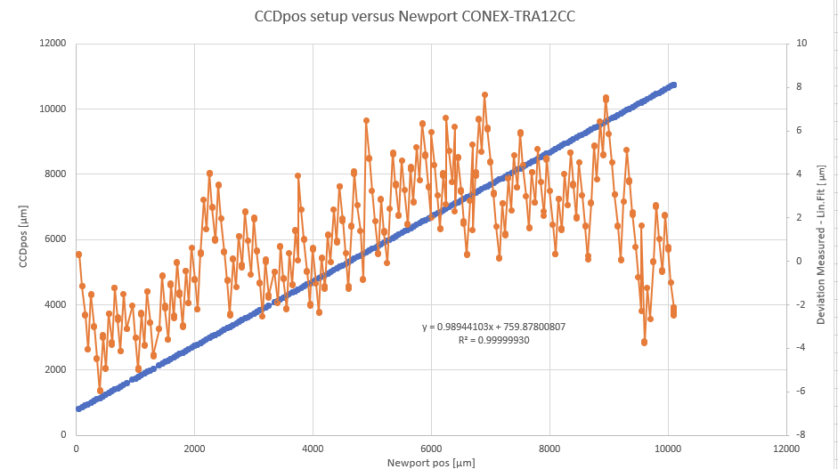 Fig 20: result of sensitivity calibration of the CCDpos setup (blue dots), incl. a linear fit and deviations (orange dots).
The linear fit shows a slight difference from the expected factor 1.000. But looking at the mechanism of the linear actuator it is quite hard to believe it has such error, certainly not over a range of 10mm. On the other hand, the relation of displacement and element-number with a lithographic defined pitch of 8um is also not a probable source of 1.1% deviation.
BUT: the CCD readout mechanism is driven by clock-signals from the MCU, which also drives the timing of the ADC that converts the analog signals from the CCD. Because all timing in the MCU is derived from one main clock there is no chance of frequency mismatches. Conclusion: I don't understand why I measure a 1.1% difference.
The second plot is a complete different story: here the influence of signal handling, noise, the stability of the laser beam and the robustness of the readout software has a contribution to the accuracy of the measured displacement. I definitely must repeat this calibration measurement after all kind of improvements have been implemented. The variations in the orange plot should be reduced significantly, while I expect no or a tiny change in the sensitivity figure.
Calibration and sensitivity revisited.
The measurements and the conclusions I drew are from some time ago, when my project still was developing. In the recent weeks I made various improvements on hardware and software. Initially the control for the my laser was simply adjustment of the supply voltage. To improve this, I created a small circuit based on the Howland current source, to switch to current control instead of voltage control. When I incorporated this circuit in the rest of electronics, I decided to feed both the opamp circuit for the analog conversion of the CCD signal and the laser supply with a well defined DC supply. This choice appeared not as simple as I thought, only after some investigation I found the cause of the strange phenomena I encountered. The housing of the laser appeared to be connected to the positive supply lead! This gave conflicts with other parts of my setup, especially the MCU that receives its power from the USB connectors, so my desktop PC. I solved this issue in a rather crude way: I supplied the 5V power for the laser circuit by a small isolated 5V/5V DC-DC converter. Because this converter is un-regulated, I added some capacitors at the input and output side, electrolytes for the 'big' effect and ceramic C's for fast signals.
Another improvement was the new wiring from the MCU and my opamp board to the CCD-board. Now I apply two shielded wires, one for the power and digital signals to drive the readout and one just for the signal from the CCD to my opamp board. Together with the addition of some capacitors around the opamp, the quality of the signal that is digitized has improved significantly. This was best visible in the base-line, that represents the dark-current level of the TCD1304.
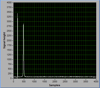 Fig 21: a graph of the data received from the MCU as example of the current signal quality. The short peak left is the Marker, the right peak is the signal of the laser spot.
Although I have plans to start a separate project to investigate simple optical setups for a nice, stable and adjustable laser beam / spot in the future, I already created some improvement in the width of the laser spot by simply placing a DIY collimator just after the exit of the beam from the laser housing. This "collimator" was nothing more than a very small ring, probably meant for a bolt of 0.8 or 0.9mm diam. I found just one on this size in my rich collection of old stuff and managed to glue it on top of a somewhat bigger ring (for M2), which became glued to a M4 ring.
The summed effect of all improvements becomes visible in my last measurements of the noise level of my readout. I created a special version of my readout application to measure the quality of the determined position. This kind of measurement should be performed in a dedicated test area where the influences of the environment are eliminated or reduced as much as possible. The main source of errors from the outside is the platform the CCD-pos setup is placed on. From experience in my working life, I know that measurements on the level of microns (um) and lower need a lot of care and precautions. As a former collegue stated: "on the sub-microm level all materials act like chewing gum". Even under relative small forces, rigid constructions may show deformations on the micron level and may vibrate with amplitudes in that region. At first it looked like I entered a whole new world of mechanics, later on I started to get used to it, but it still fascinates me.
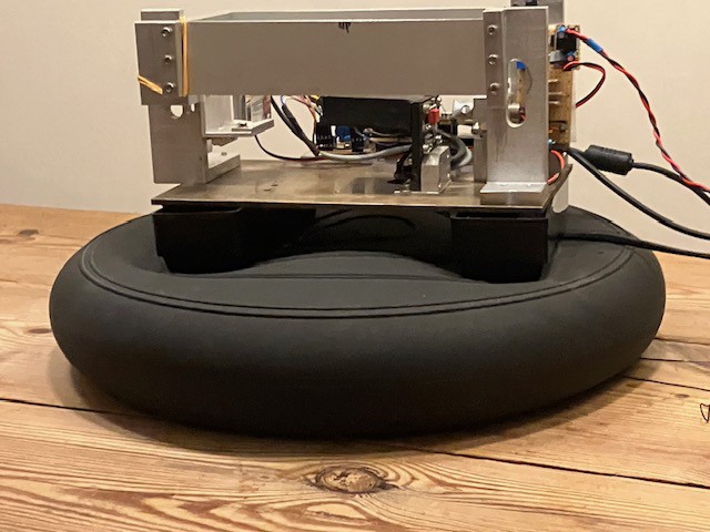
Fig 22: the CCD-pos setup placed on a air-filled cushion as primitive suspension.
Another source of disturbing vibrations is the so-called 'microphone-effect': a construction can pick up vibrations from sound in the surrounding air. Certainly when the construction has large surfaces, the fast changing differences in air-pressure we name 'sound' may induce minute fast changing forces that can result in fast deformations with tiny amplitudes.
I decided to apply a trick to make a quite arbitrary separation between changes in the measurement output due to the environment and due to the setup itself. The reasoning is that the disturbances from the environment are mostly in low frequencies and the remaining amplitudes come from imperfections of the setup itself.
To create a simple mechanism that can be run real-time during the readout of the CCD plus the signal handling, I chose to smooth the derived signal with a qubic spline fit. This smoothed signal is assumed to be representative for the influence of the environment. When I subtract this signal from the original measured data, the outcome should show the imperfection of the setup itself.
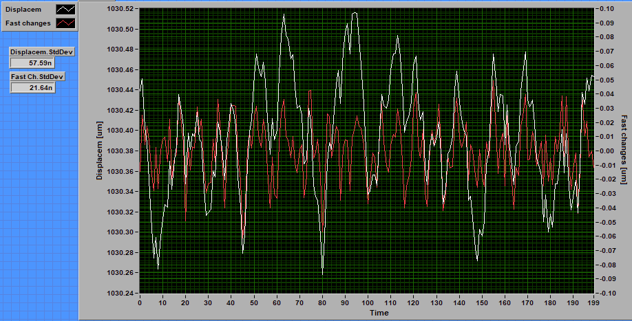 Fig 23: graph of measured signal (white) and result of measured minus smoothed signal (red) against time.
I calculated the StdDev of both set values (200 points each), see at left in Fig 23. The value for the 'Fast changes' suggests that 63% of the readings with my setup (positioned on a table in my living room) deviate 21.6nm or less from the exact position. I must admit I have selected a period without obvious peaks from external origin, like footsteps, bumps to the table, etc.
Future plans.
At this point I stop writing and will change the status of this project description to 'public' so the whole world can see what I wrote. This doesn't mean I stopped the development nor I will stop writing about the CCDpos project. There are still quite some subjects I consider interesting enough to describe and may be useful for other technical hobbyists.
As this is the first time I create a project on Hackaday, I have no idea how to publish additions or comments on a project, maybe other users have ideas and/or suggestions?
Anyway, to be continued........