I already have the LED board ready. I proceed to design the driver. According to the assumptions, the driver will have the ability to change the brightness of the LEDs for each channel (cold, warm and neutral).
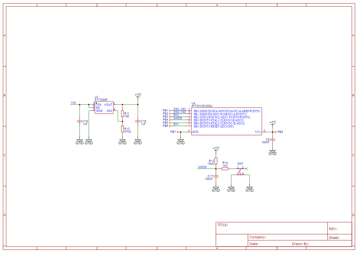
The original lamp has a function to change brightness in three steps. I have not reverse-engineered the entire design, but it appears that a PWM signal is responsible for adjusting the brightness.This waveform is generated by an Attiny25 microcontroller. Also in my modification I will use exactly the same microcontroller.
As the main driver, I decided to use the LED5000 chip from STMicroelectronic.This circuit is a current source (step-down converter) with a current capacity of up to 3A controlled by a PWM waveform.Depending on the PWM filling, we get different current values at the output of the chip.In this way, we can adjust the brightness of LEDs.
Cold and warm color temperature LEDs draw different current values. Therefore, I will need two such current sources. Separating the control of the channels (cold/warm) will make it possible to compose your own brightness ratios in the future.
Below I present the first version of the schematic. To design the schematic, I used the datasheet provided by the manufacturer and the eDesignSuite web application as reference.
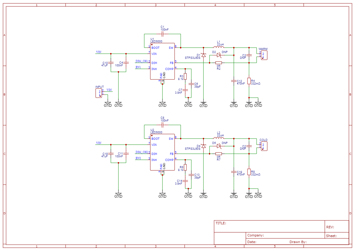
The producer pays special attention to the value of capacitor C12 and C19. As a result, the light flicker will be at an unacceptable level. We will see how it will work during testing.
The circuit of the driver is quite simple and does not need to be discussed in detail. The main circuit U1 is the current source mentioned earlier. Capacitors C10, C4 are responsible for filtering the input voltage. The Vin voltage is supplied from the original power supply with an output voltage of 21.5 V and a current of 1 A. The U1 circuit support ceramic capacitors at the input and output. The ceramic capacitors in this case have the appropriate voltage rating. Capacitor C1 amplifies the gate driver of the internal MOSFET transistor above Vin to fully turn it on. This minimizes conduction losses in the power switch to maintain high efficiency.
Elements D2, R2 and R4(Rs) create a simple overvoltage protection. The external compensation network consists of elements R3, C6 and C7. It is connected to the error amplifier output (COMP, pin4) to stabilize the system according to the application conditions. Parts L1 and D1 form the basic step-down inverter topology.
The circuit was duplicated for channel two.
The controller also consists of the aforementioned Attiny25 MCU, which is labeled U4 in the schematic. The tact switch for changing the mode is connected to the microcontroller. Elements R13, R14 and C17 are responsible for eliminating vibrations of the button's contacts (stabilizing operation). The microcontroller requires a supply voltage of 5V. This voltage is generated by the U3 - ST730MR stabilizer.
Discussions
Become a Hackaday.io Member
Create an account to leave a comment. Already have an account? Log In.