 RATelectro
We didn't expect this, but our humble GitHub was discovered by PCBWay, and they kindly offered to sponsor several boards for our project. Since we already had some sketch of our pedal enclosure in 3D, we took all our previous schematics and developments with the stacking layout and, within a few weeks, designed new boards for this enclosure. It was a fast-paced effort, but it served as a good stress test for our team, inspiring us to pay more attention to our publications and the project as a whole.
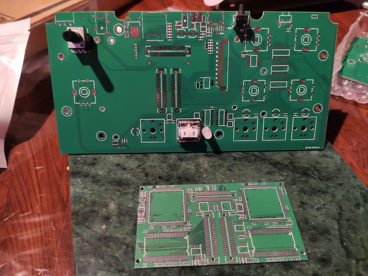
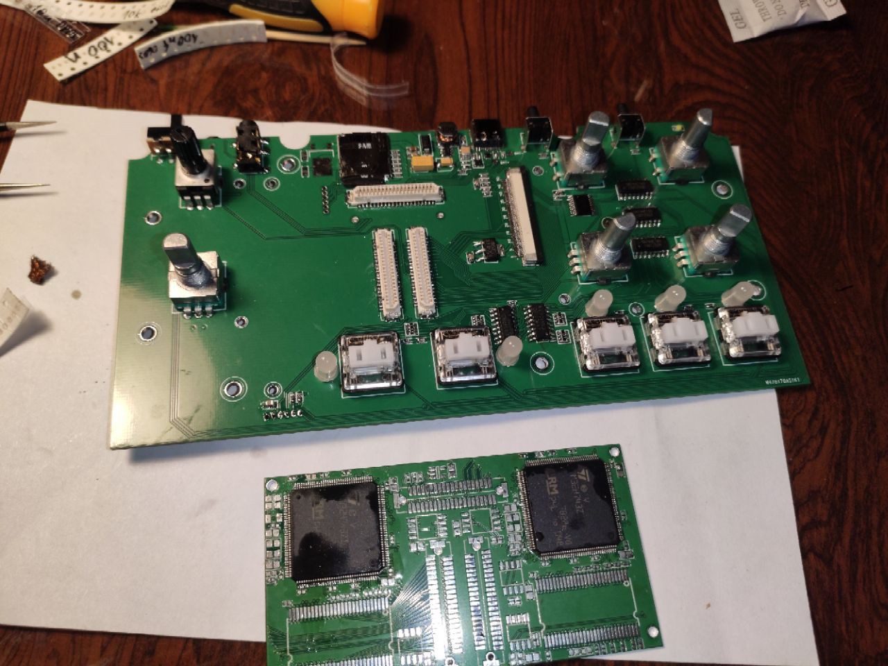
— We received the MCU boards and Main boards from PCBWay, as well as the Codec, Audio Connectors, and FootSW boards from our local PCB manufacturer.
Packaging
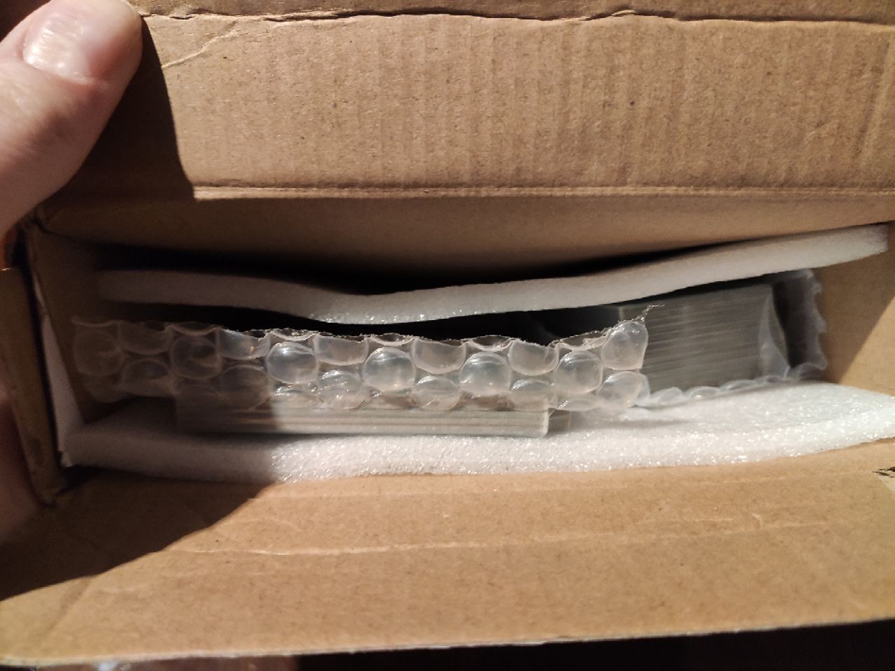
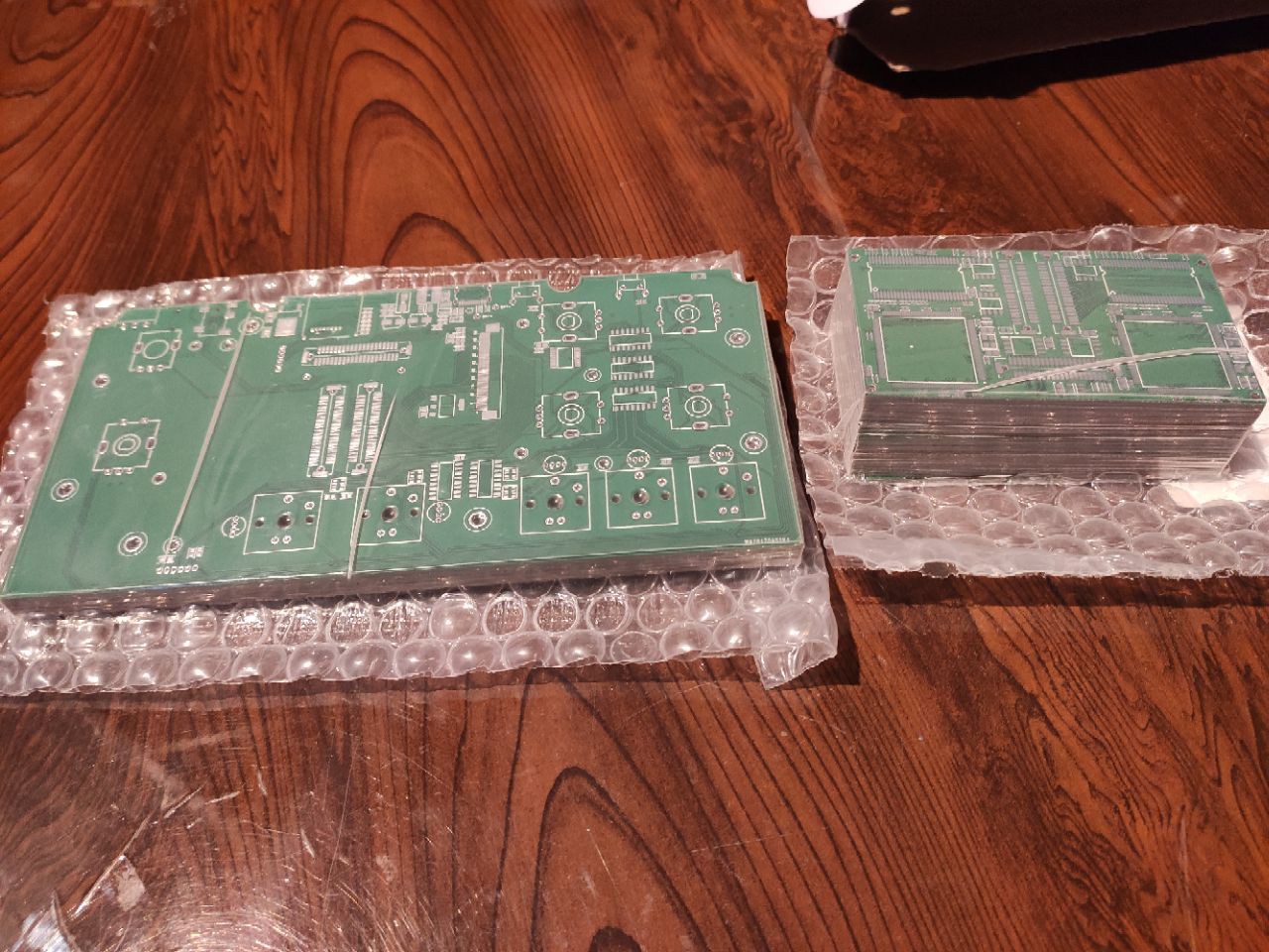
The package from PCBWay is kind of most PCB manufacturers standard, but nice for the price - branded box, some foam inside, and most importantly, all PCBs are vacuum-sealed in bubble-wrap, which prevents them from flying around and rubbing against each other.
The package from our local PCB manufacturer (we use express build and delivery option which gives us one and a half week from order to solder) for small-scale PCBs looks like a branded A4 format envelope, covered with bubble-wrap inside.
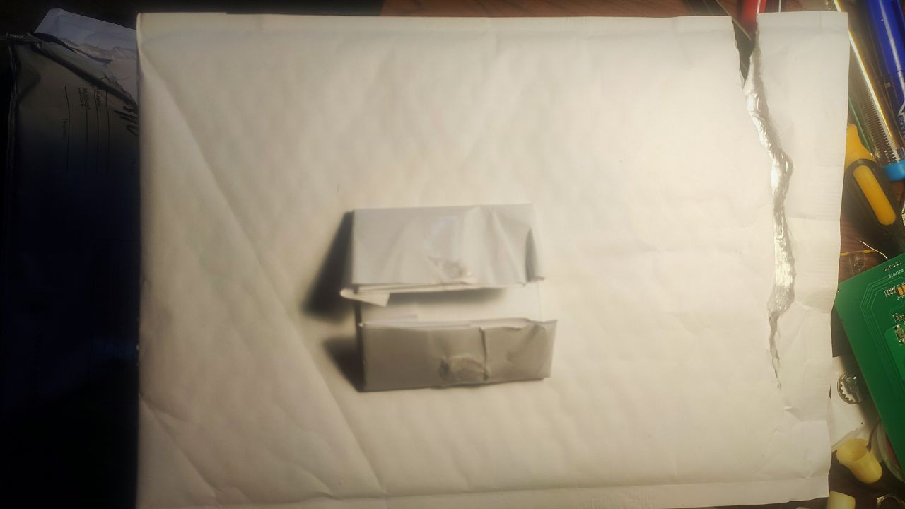
What goes inside is not always consistent and depends on board complexity and their quantity. Simplest 2-layer boards with tiny size can just be poured inside with no additional protection. In most cases though, they provide boards sandwiched between pieces of plywood, each covered with paper to prevent rubbing, which is nice. In our case, well... We just got them hand-wrapped inside some A4 paper with tape. Honestly, this is the first time I get boards in this kind of "package" from them, and it is Ok for simplicity, quantity and purpose of my PCBs, but it is not Ok for me)
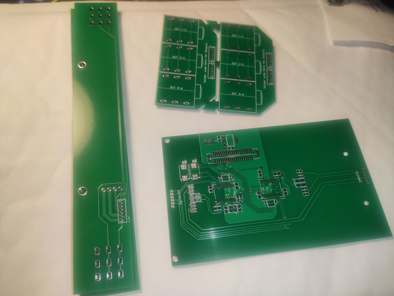
Boards
Now we can evaluate the quality of the boards and take look at them in more detail. Let's put them under a microscope! But before this, I have to say that it would be unfair to compare these two manufacturers today, because we got completely different boards from them with different specs and number of layers, but rather just observe some eye-catching details and possible differences that can be noticed.
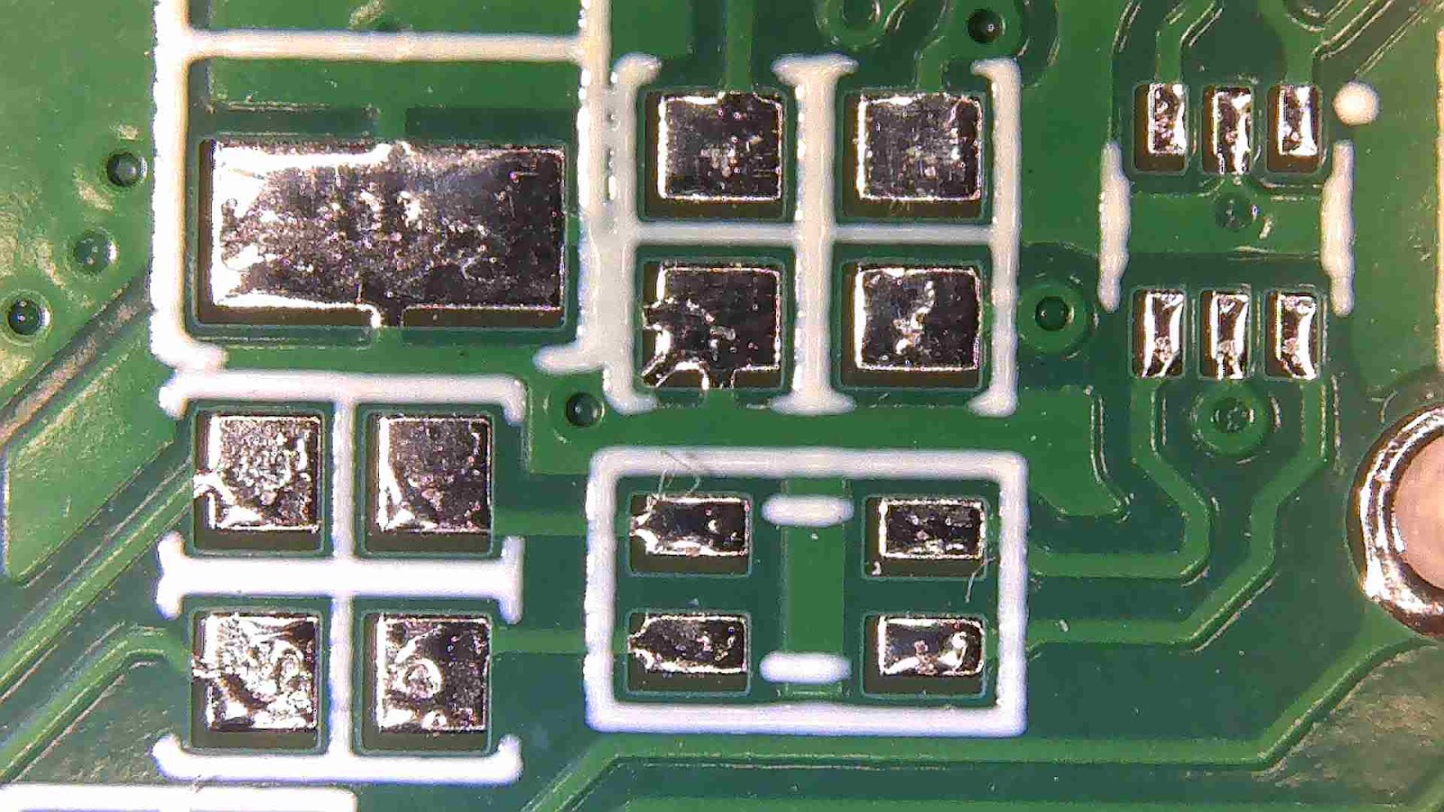
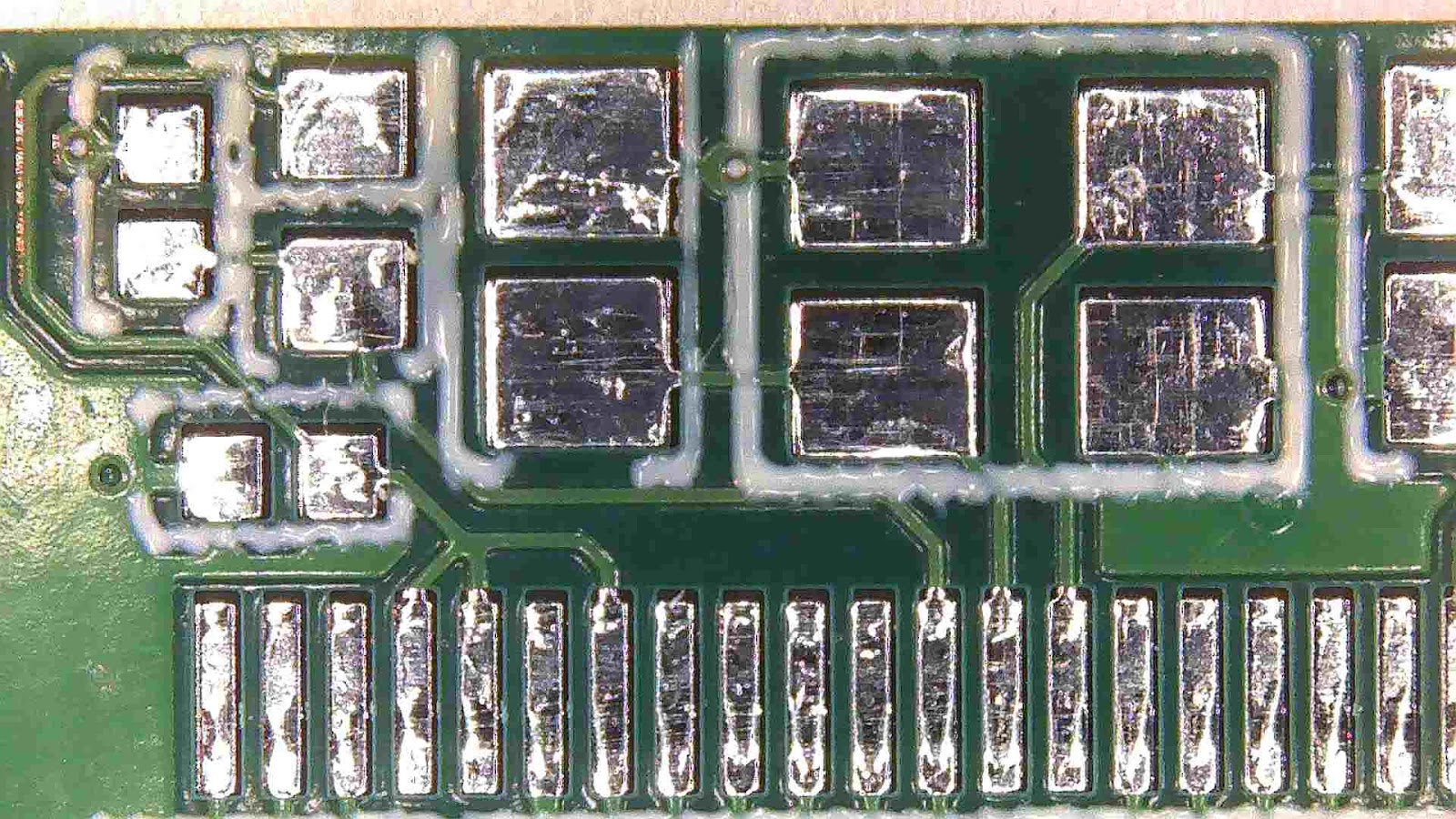
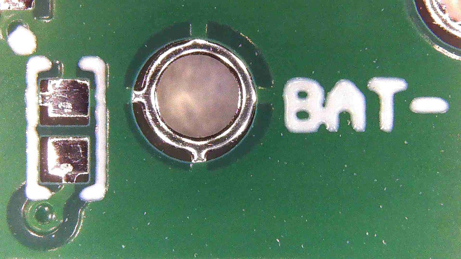
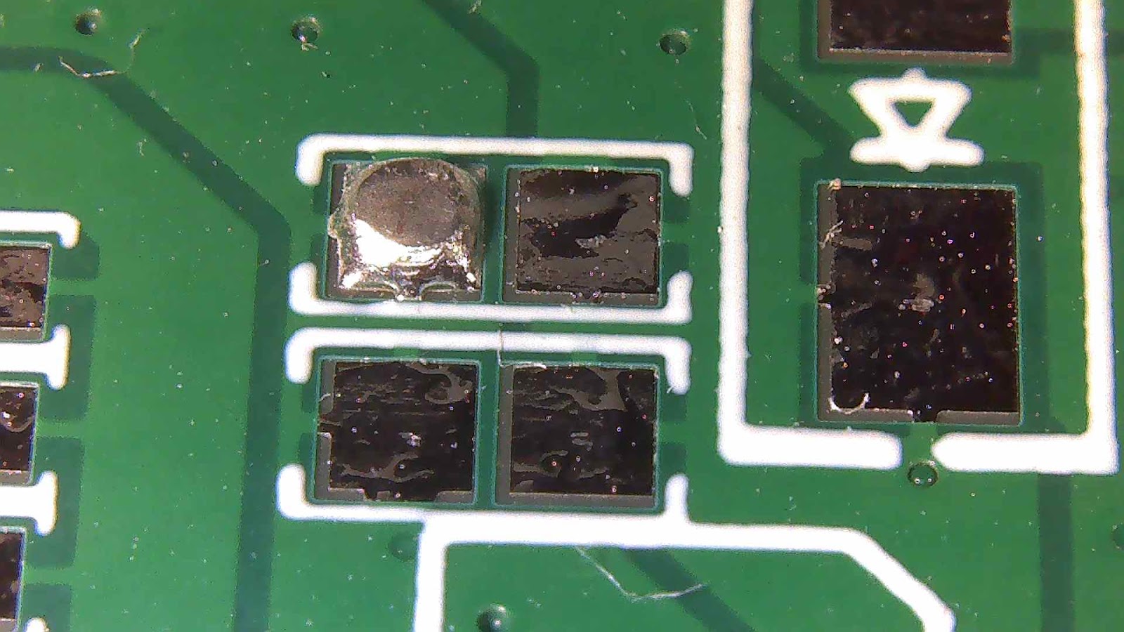
On PCBWay 2-layer boards, we can first see some solder mask misalignment with all the pads. It is not too big, but noticeable for smaller pads like on picture above. it is also fixed in size and direction along the boards and across them, all the pads fit into mask openings, so I guess it should be Ok for 2-layer lowest-tolerance boards.
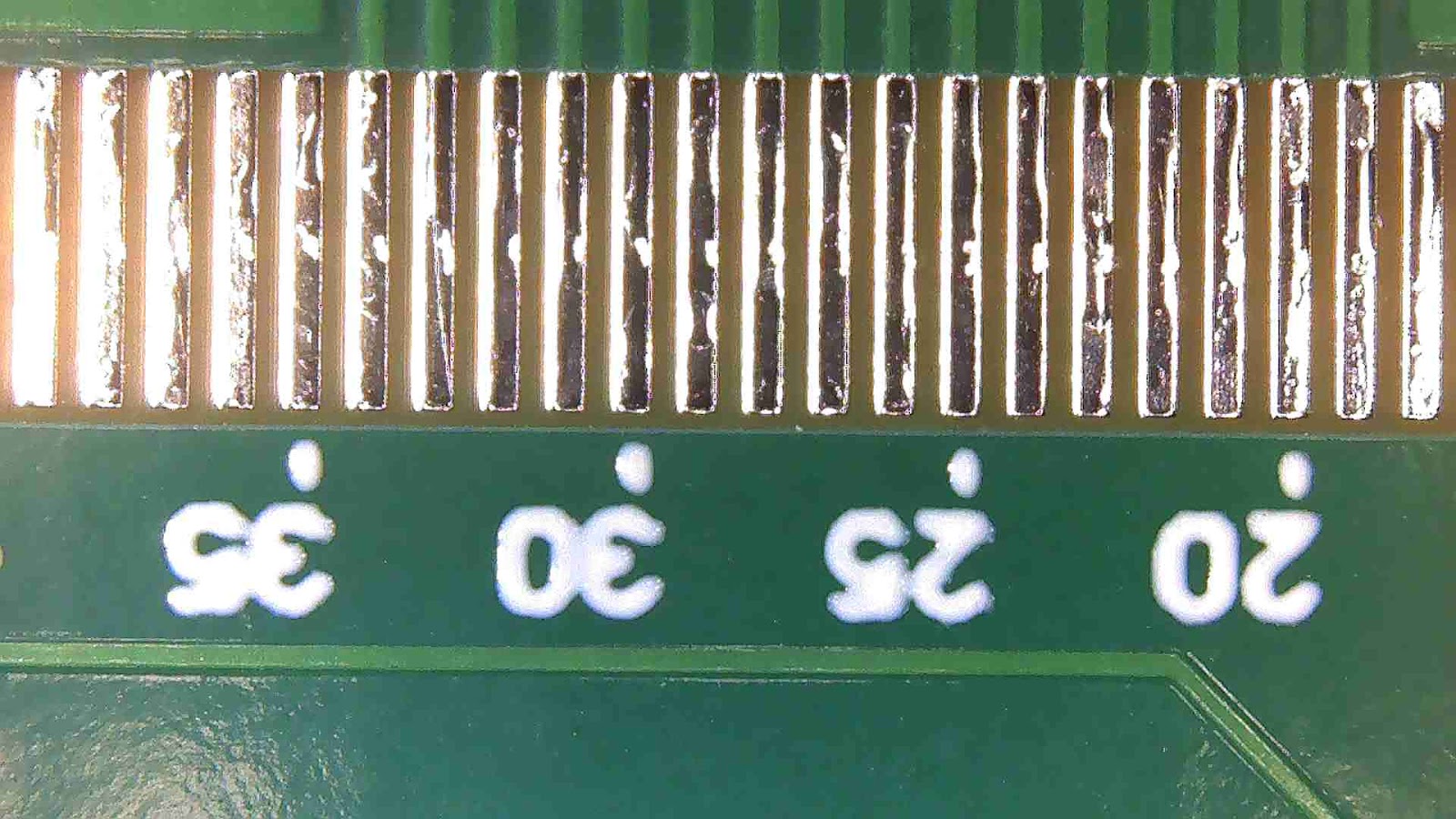
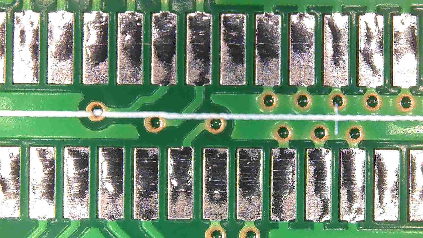
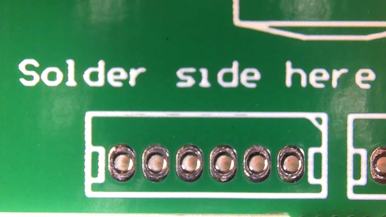
The silkscreen is not the best but readable, you can notice it has some wobbliness in one direction:

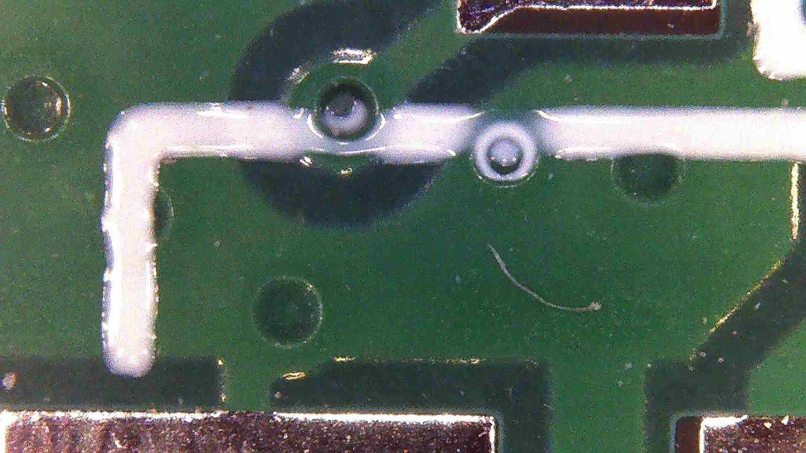
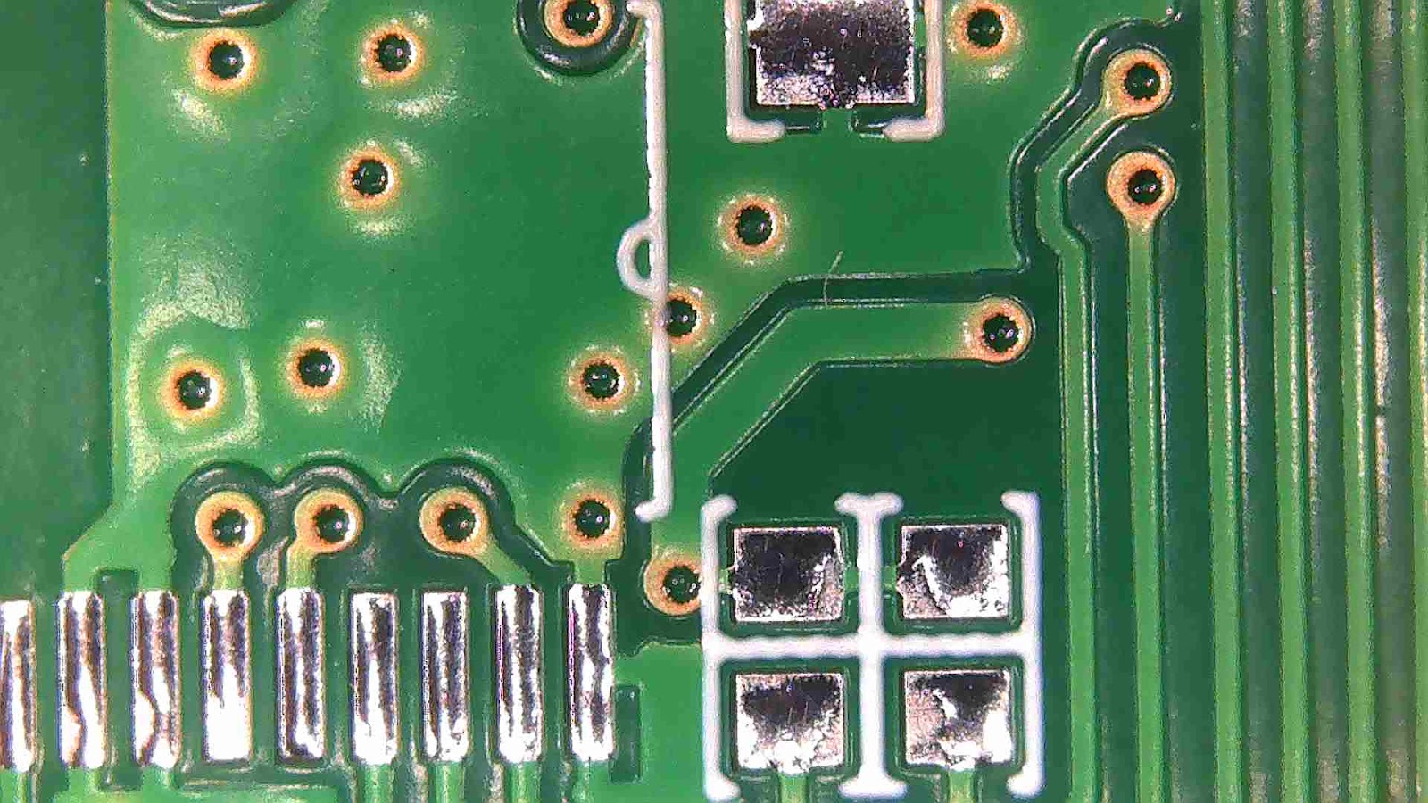
This is a higher tolerance 4-layer board - solder mask tolerance is also higher, but still a bit misaligned.
Interestingly, I noticed that some VIAs have a slightly different shape than in my CAD. They seem to have been enlarged wherever possible and then trimmed to ensure minimal clearance is met. This gives more room for drill holes, as they always have some positioning error. Most likely, this is the result of post-processing my gerbers by the technicians or their automatic software, as on the MCU board, I used the smallest possible VIA sizes of 0.4/0.2 mm. On the main board with bigger and easier to manufacture VIA size 0.6/0.3 mm, they all look round.
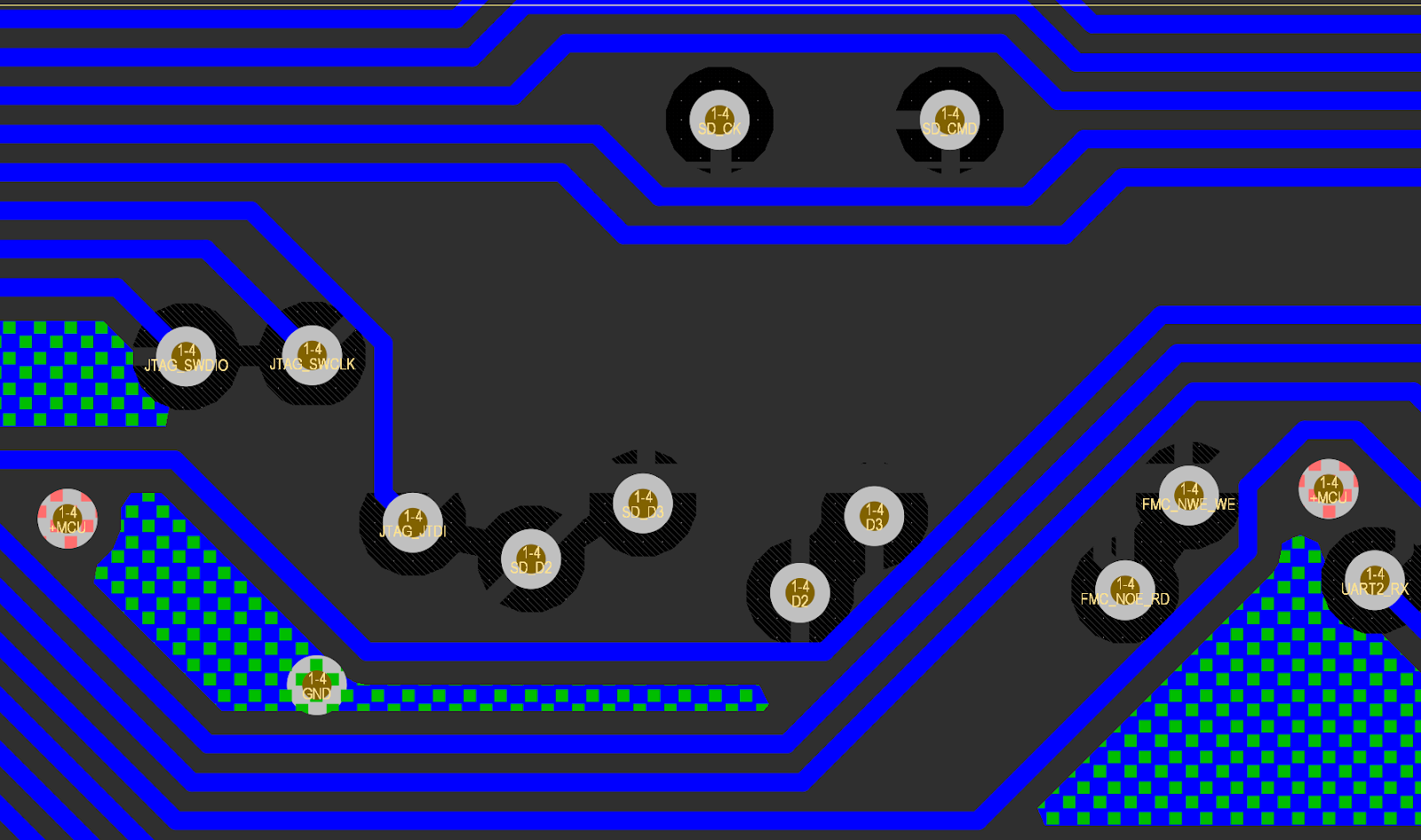

Although, out of all the boards, this only happened on one. I hope it's just a drawback of the inexpensive manufacturing process, and for serious serial orders, more careful control is in place.
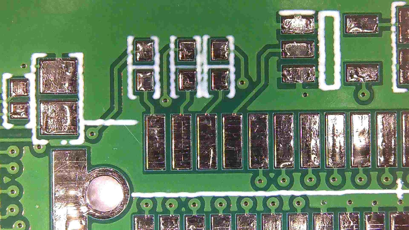
As for our local manufacturer, we can see that their standard solder mask is kind of more liquid and thin, which allows to make much smaller mask opening and wider sliver, but in expense of poor VIA cover:
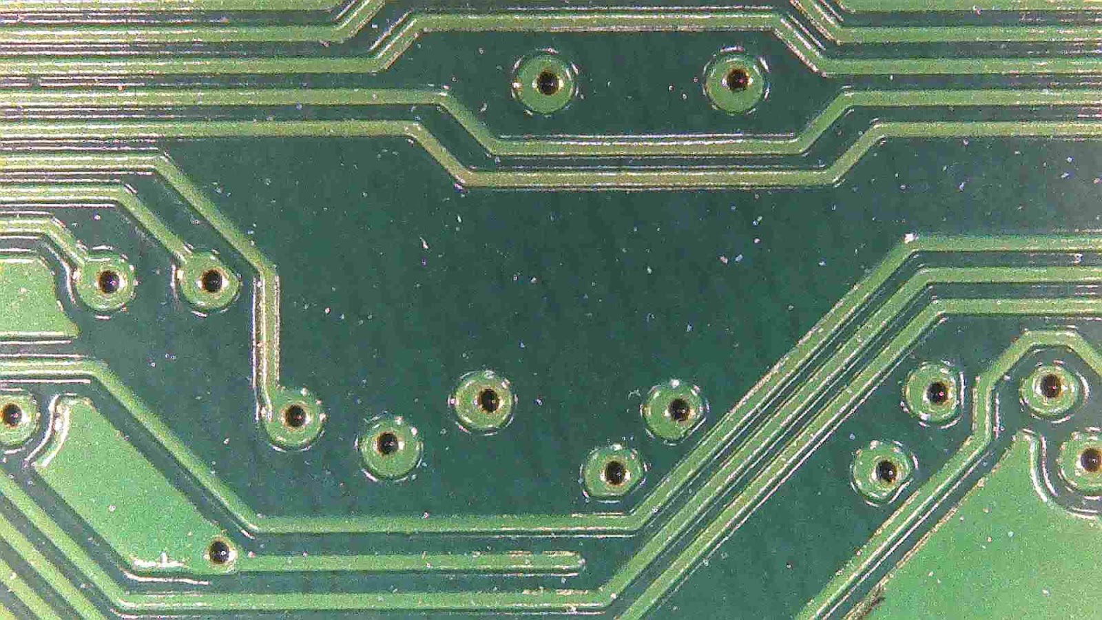
The silkscreen is good, the line wobble is still there, but is barely noticeable:
Other than that, I haven't noticed anything special - just simple 2-layer boards, as one would expect, but with huge labour and engineering fee for their simplicity, as a downside.
Conclusion
All in all, aside from differences, both manufacturers satisfy our need for good quality PCBs for our project. All traces and pads on all boards seem fine, and solder mask and silkscreen issues do not affect boards functionality. PCBWay's boards are good value for the price, and are just what we need for our project.
Discussions
Become a Hackaday.io Member
Create an account to leave a comment. Already have an account? Log In.