See also this YouTube video describing the way the system works:
This is my attempt at making a fast 6502-based homebrew computer. The current prototype is stable at 32.768MHz, which I'm happy with as it's in the same ballpark as 6502.org forum user "plasmo" has achieved in the past - I believe he may have had 40MHz working. 40MHz doesn't work for me, and I haven't tried any frequencies in-between yet.
Full schematics for the current prototype are linked below and in the "Files" section, and I will see about providing code and PCB designs when I find the right way.
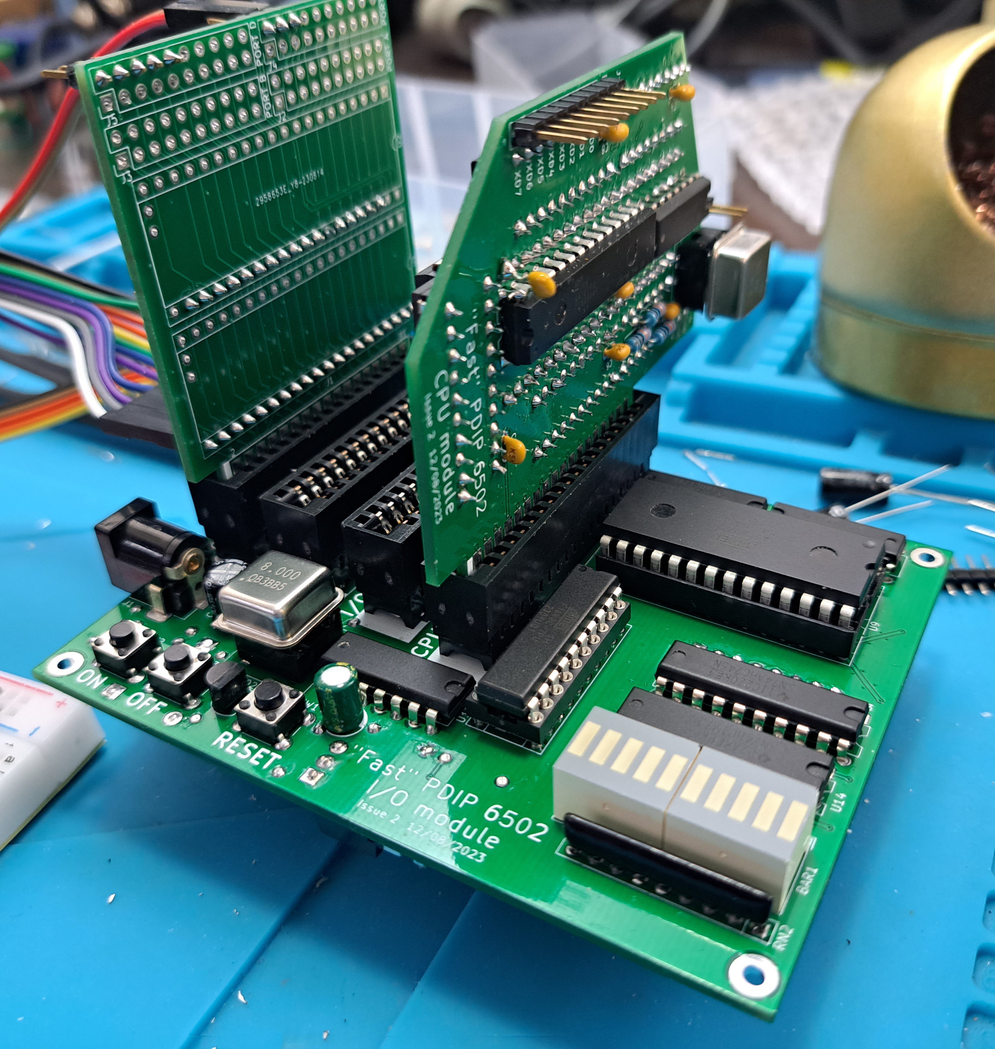
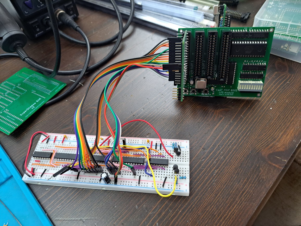
Here's what the system looks like fully assembled, with the CPU module present and an expansion card in place. I used a modular design so that I could iterate on modules individually without having to rebuild the whole system each time, and add more modules at later dates.
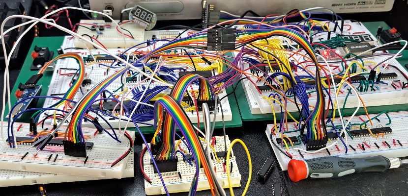
And here's the 25.175MHz breadboard prototype, with more work-in-progress - see below for more details on that:
Concept
I've built several 6502-based computers over the years I've been learning electronics, but my focus has never been on clock speed except where it was necessary - I've been more interested in designing peripherals, such as video output cicruits or floppy disk controllers. Nevertheless I've had a design in the back of my mind for this, and I decided to flesh it out and build it.
The main principle is that the only bit that really matters is how fast the CPU can run from RAM, so we connect them together as directly as possible and don't accept any compromises for the sake of other components. While many similar systems tend to run code from ROM, this is not essential as you can generally just copy the code to RAM before running it - and in any case you can still run code from ROM, just more slowly. Similarly, I/O operations are rare compared to RAM operations, and it doesn't matter much how slow they are.
In practice this allows the computer to run at over 25MHz on a breadboard, and over 30MHz on a PCB, and although I/O operations are slower, in practice they are so rare they don't affect the average clock speed much.
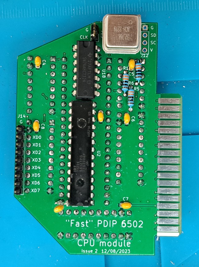
CPU Module
 |  |
Schematic: https://cdn.hackaday.io/files/1926308241481920/6502fast3cpu-iss3-schematic.pdf
Removing ROM and I/O from being core considerations enables us to design a tighter core system consisting of the CPU and the RAM directly tied together with a fast clock. This CPU module is essentially a self-contained 6502 computer system, and mostly runs on its own, but lacking non-volatile storage, it can't actually boot itself. To communicate with ROM and I/O peripherals then, we send a signal to an I/O module, and hold the CPU clock high - pausing the CPU mid-instruction - until we get a response saying the operation is complete. The CPU's buses are buffered from the I/O module using bus transceivers, to ensure that the core CPU/RAM combination is as unencumbered as possible in normal operation.
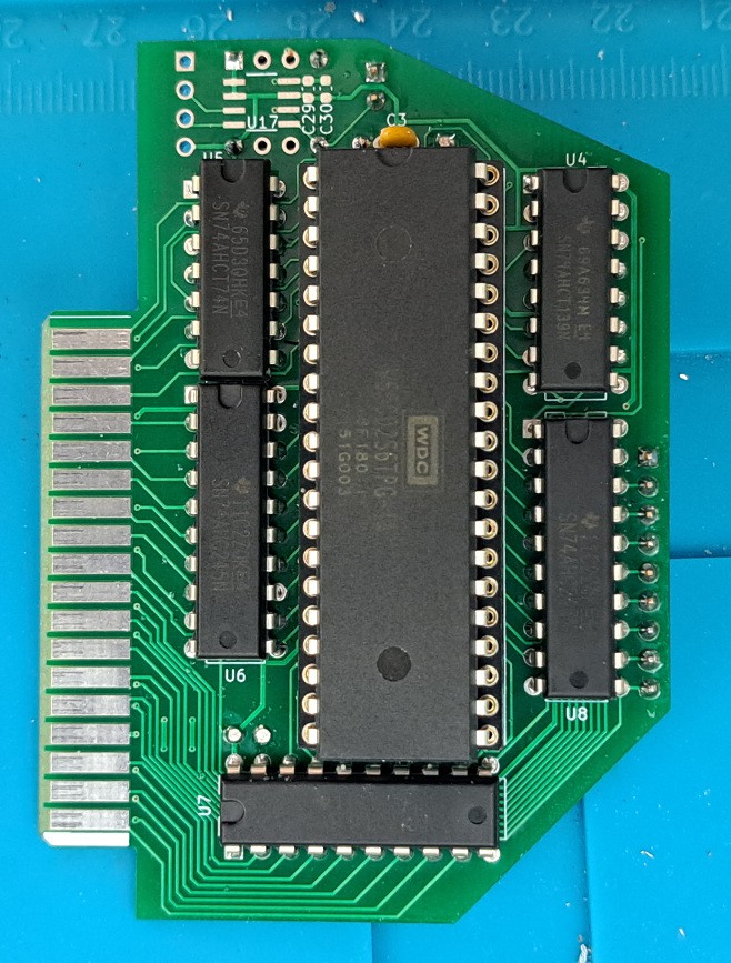
I/O Module
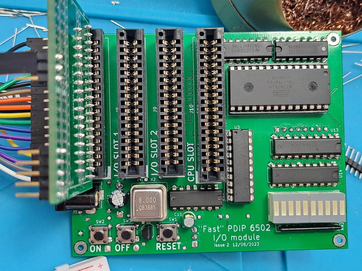
Schematic: https://cdn.hackaday.io/files/1926308241481920/6502fast3io-iss2-schematic.pdf
The I/O module handles all operations other than fast RAM access. Examples of I/O operation include accessing a 6522 VIA's control registers, setting an LED state on a debug port, sending a byte over a serial link, or reading a byte from ROM. It forms the bulk of the system, and is architecturally very similar to any typical 6502-based computer system - just without direct connection to a CPU.
It receives the "IOWAIT" signal from the CPU module, along with the address and data bus states, and performs the usual type of address decoding to decide which I/O device (or ROM) should respond to the request. The device in question then needs to do that based on the address and data bus states. When the device is ready, the I/O module can send the "IOREADY" signal back to the CPU module to unpause it and let it carry on.
In theory we can wait for different amounts of time for different peripherals, but to simplify things a bit I decided to run the whole I/O module at a consistent clock rate, using its own clock oscillator. This is beneficial for components like the 6522 VIA, which include hardware timers that don't make much sense if you let the clock speed vary; and it makes the general design of the I/O module very close to the usual way 6502-based computers are built, just without a directly-connected CPU.
Crossing clock domains
It may have been possible or even better to derive the I/O module's clock from the CPU clock, by dividing it by 4, 8, or some other value. However, I decided not to do this, because at least in the prototyping stages it's helpful to be able to vary the CPU clock speed at will without having any impact on the I/O system. If the system becomes unstable as a result of changes to the core clock speed, I know that it is entirely due to the CPU module, and not due to secondary effects on the I/O module.
However, using multiple clock domains creates some complexity. Whenever a signal such as "IOWAIT" crosses clock domains, it needs to be synchronised to the local clock. Typically this is done through one or more D flipflops, usually two, to minimise risks of metastability. If the I/O clock had been derived from the CPU clock then this wouldn't have been necessary.
It is possible that at some point I'll switch to a derived clock, but for now the design works well like this and there are benefits to the separation.
Pluggable I/O Submodules
The I/O module functions a lot like a PC motherboard, and it already includes some I/O devices - a ROM socket for the system to boot from, and a simple eight-LED debug display. It also has a 74AHCT138 8-way decoder to support more I/O submodules. The LED display is device 7, and there are three card-edge sockets on the board into which devices 0, 1, and 2 can be plugged. These slots have essentially the same pins as a 6522 VIA, plus a few extras that may be useful for some device types - for example, an additional address line and its inverse, allow two VIAs on one board.
In addition to the original VIA submodule, I have built some other I/O submodules on breadboards for serial I/O and SD card I/O. It's pretty easy to design them, especially as they only need to work at <10MHz, and quickly adds a lot of capability to the computer.
Miscellaneous niceties
Finally there are some necessary and some nice-to-have features - a power jack, on/off/reset buttons, breakout headers for the critical CPU signals to allow probing or connection of a logic analyser, and although this is a PDIP project, there's an SMD footprint for a programmable oscillator to allow trying out different clock frequencies without needing specific crystal oscillators.
Breadboard Prototype
Before getting the PCBs made, I prototyped the design on a breadboard, to check it was going to work. It did work, and much faster than I expected the breadboard to achieve - it's stable at 25.175MHz, surviving a lot of stress testing. Since getting the PCBs made, I have used the breadboard prototype to explore changes to the base circuit, as well as to develop and test add-on I/O submodules. Here it is in its current state - very messy as my focus is currently on the submodules, not the main circuit itself:
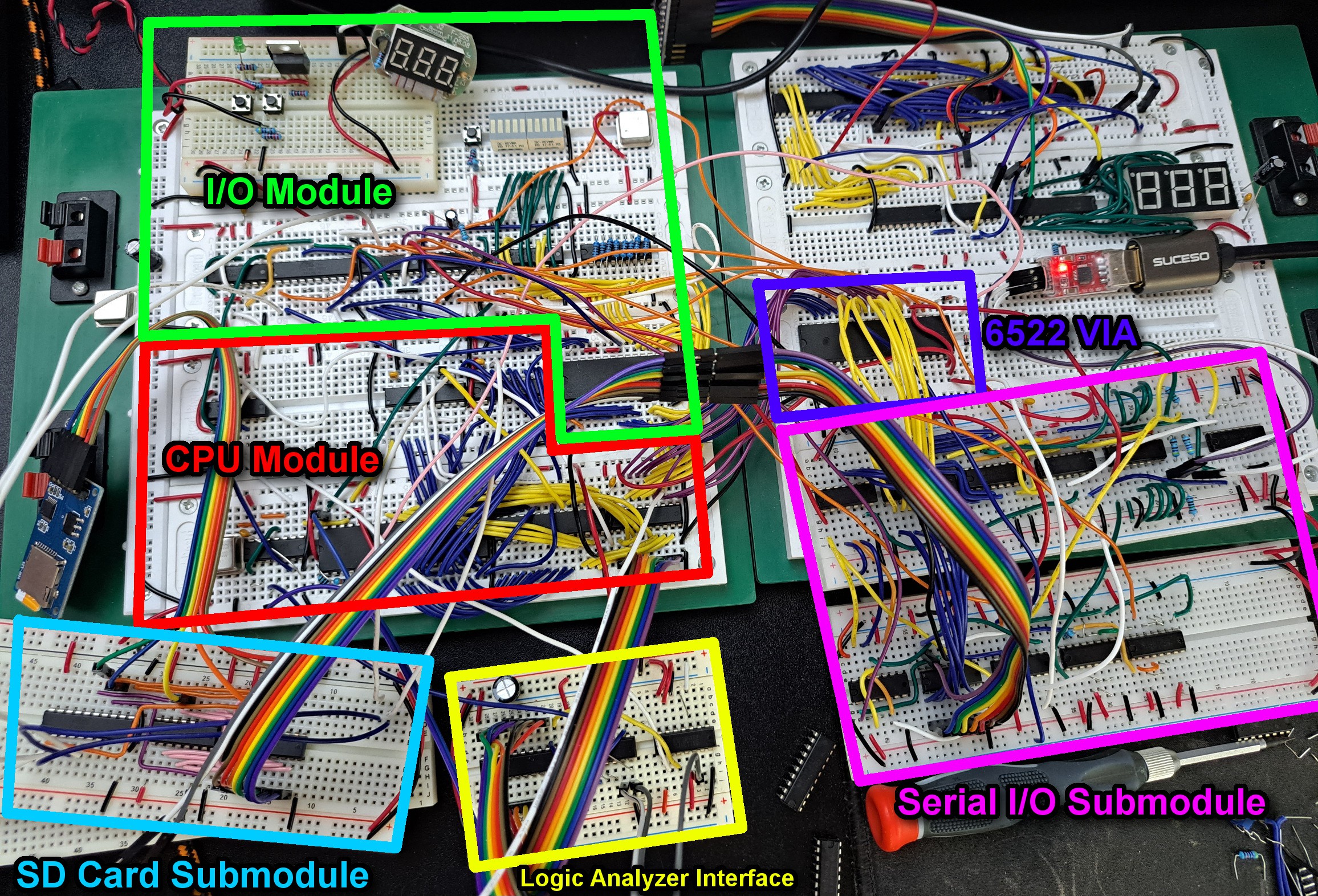
The breadboard prototype is still using an older version of my serial I/O submodule - the photo further above has the newer, 5-chip one.
PCB Design
For the PCB design, I wanted to keep costs low, so chose to initially use 2-layer board. However I wanted to ensure good signal quality, so I made one layer be a ground plane, and took care to reduce the number of places it needed to be cut, and to provide reasonable ground return paths for signals crossing the cuts. I don't know whether this is a good approach or not - I know that historically it was much more common to just route ground by hand for this kind of board.
I had considered making 4-layer versions for comparison, especially for the CPU module. However I'm not sure how much benefit there'd be - there are very few incursions into the ground plane in the CPU module, and they are very short, so maybe the only benefit would be that the ground plane would be physically nearer to the signals, rather than on the other side of a 1.6mm board.
You'll find below some layered images of the board layouts and trace routing for the CPU module and the I/O module - these are the versions I've done most testing with as of 17/10/2023. Full design files are avaiilable on github, including the gerber file zips that I sent to the board manufacturer.


Address Decoding and Memory Map
The 6502 CPU runs based on a two-phase clock, generated internally based on a single-phase input clock. It performs some operations during "Phase 1", when the input clock is low, and some during "Phase 2", when it is high. The combination of Phase 1 and Phase 2 makes up a full CPU clock cycle in which it does a block of useful work.
Phase 1 is mostly about setting up the buses to control what happens during Phase 2. Some time after the input clock falls, the CPU drives the address bus to an address it wants to read or write; and sets the RWB pin high or low accordingly. Our circuit needs to look at that address and decide what to do during Phase 2. By the end of Phase 2, we need to either fetch a value (e.g. from memory or an I/O device) or we need to write a value (to memory or I/O). In addition during Phase 2 the CPU performs some other operations - in particular in write cycles it will activate its data bus drivers and provide the value to be written, some time after the start of Phase 2.
In our system we need to decide - by the end of Phase 2 - whether we can serve up the data straight away, or whether we need the CPU to wait. If the bus cycle is a RAM read or write operation then we want to process it immediately - otherwise we want to hold the clock high, so that Phase 2 is extended while the I/O Module deals with the operation. We need to make this decision in time for the clock to be held high if necessary, or allowed to fall otherwise.
it turns out this is quite a limiting factor on how fast you can clock the system. To keep things as simple as possible here, in my initial design I allowed this decision to be made purely based on the high bit of the address - if it's set, then it's a slow ROM or I/O operation; if it's clear, then it's a fast RAM operation. This works very well.
if the operation is a slow operation then the I/O Module does further decoding on the address to decide what to do with it. It has a lot more time to make this decision, and can do a more fine-grained decode. I still wanted to keep it within the capabilities of a 16V8 PLD (plus a little glue logic) and the memory map I settled on was as follows:
- $0000-$8000 - RAM (fast)
- $8000-$FF00- ROM (slow)
- $FF00-$FFC0 - I/O (slow - 32 bytes for each of the first four I/O devices, 16 bytes for each of the last four)
- $FFC0-$FFFF - More ROM - CPU reset/interrupt vectors
The system can run with a large or small EEPROM - up to 32K. I'm investigating the possibility of using a smaller EEPROM and having fast RAM in as much of this upper address space as possible instead - given that running code from EEPROM in this system is undesirable - however this complicates thte first stage address decoding enough to restrict the speed of the breadboard prototype, and whether this is viable on PCB without hampering the clock speed remains to be seen.
Software
The system initially boots from ROM. I have various ROM images in use at different times - firstly a variety of small test programs to exercise the system and reveal hardware bugs; then a growing Operating System, which starts by copying itself into RAM to run faster from there; and finally a lightweight boot monitor which waits for commands from a PC attached via USB Serial cable, usually involving the PC streaming code for it to write into RAM, and then execute. The latter is the quickest way to develop, but requires tethering to a computer.
All the code, build scripts, PLD sources and PCB sources are in the github repository: https://github.com/gfoot/fastpdip6502
64K RAM upgrade
I've been experimenting on the breadboaord prototype with increasing the amount of RAM to 64K and reducing the amount of ROM to only a few hundred bytes. In this version the ROM starts at $FE00, with everything below that point being RAM - and the I/O window is unchanged. The ROM space is then only large enough to hold a bootloader of some kind - though it would be possible to allow paging in other areas of the much larger ROM IC.
This is working very well on the breadboard at 25.175MHz. I mostly use a serial connection to load code into RAM, with the ROM bootstrapping the process. I also have a bootloader that boots from SD card. On the whole it's a nice change.
However it is now much harder (slower!) to decide whether a bus cycle is fast or not. To decode addresses below $FE00 we need to decide based on the top seven bits of the address bus, not just the top bit. To do this I'm using the fastest PDIP PLD that I know of - ATF16V8C-7 - and it is working, but I'm conscious that this decode time is on the critical path and it may impede the faster clock speed of the PCB version. So while it may make for a better, more flexible system, it is against the main goal of this project which is to run as quickly as possible without compromises.
I will need to make some PCBs to try it out.
Any questions or comments?
Please do share any questions or comments - there are more files I should upload and share but it takes time to get them together. If there's anything you're particularly interested in though, please do say, and maybe I can either explain or share it sooner!