 Keith
Keith2023-10-14
After a lot of reading and feeling like D.P. Gumby saying "My brain hurts!", I've now got a better grasp of what is going on.
I started from Andy's ZX81 logic in TTL. You might think "surely that is just a ZX80" but it is isn't. The ZX81 had to pull many tricks to fit the logic in a 40-pin ULA. Extensive "resistorplexing" of course, but it also had to make do with a limited number of Z80 signals. The ULA had to find different ways to know where it was in the video display cycle.
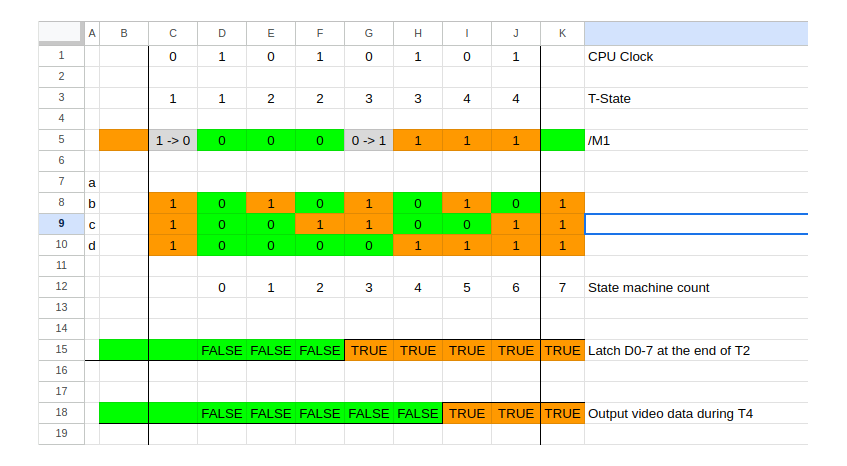
Andy's TTL replacement for the ULA used a state machine based on a 3-bit counter, reset at the start of /M1 and clocked twice the CPU clock rate. The logic can then know where it is in eight phases of T-states 1 to 4.
In the ZX80, the video character latch is loaded at the end of /MREQ when not refreshing, and read when /RFSH and /MREQ are low.
In Andy's TTL ZX81 logic, the video character latch is loaded at the end of T2, and read during T4.
For character text display, the video character latch drives address lines of the font ROM.
For G007 graphics display, the process is very similar but the latched video data is read straight to the data bus without having to go through the font ROM. I think the load and read signals could share the same timing, but with the font ROM disabled during G007 graphics and vice versa. This bodes well for integrating G007 graphics into Andy's logic.
2023-10-15
Andy's state machine seems to begin by clocking in /M1, which falls slightly after the start of T1.
I am not sure about the start and end conditions, but the display process is the above repeated 32 times. So the end of one becomes the start of the next.
Andy's logic seems the best for TTL implementation.
I wondered if the state machine in GAL chips could be optimised like so:

Here the state machine includes the latch's clk and oe signals, which saves needing separate pins.
The machine stays in state 5 (idle) unless /M1 is low, in which case it cycles through states 4,6,3 and 5.
The latch output may only go low for video cycles, so the simplest fix may be to clock /M1 in during video display (A15 and A14 are high).
2023-10-19
After correspondence with Andy, I see I have made two errors
- Andy's state machine enters state 0 asynchronously as soon as /M1 falls.
So the timing begins half a clock earlier. - ZX81 ULA replacements have to load the character latch BEFORE forcing NOP on the data bus,
unlike the ZX80 which does both at the same time.
Thus the timing looks more like this:
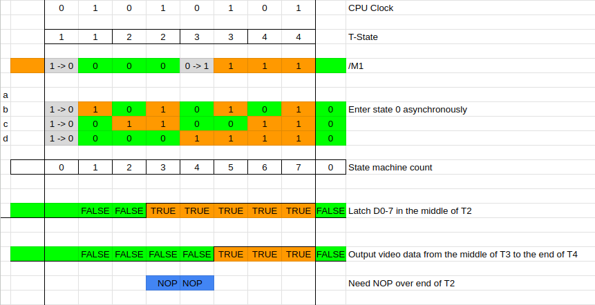
The forced NOP has to straddle the end of T2. It needs some delay to allow the data hold time of the data latch, and some delay between releasing NOP and the data latch output enabled.
One can do this with gate delays, or double the clock resolution and have the forced NOP just a quarter of a CPU clock cycle either side of the end of T2. Andy says his Xilinx version of the ULA does the latter.
Discussions
Become a Hackaday.io Member
Create an account to leave a comment. Already have an account? Log In.