 Dave Collins
As I wait for PCB's to arrive from PCBWay's factory in China, I thought I would spend a few moments to go over the general architecture of the computer. We can start with a simple memory map:

The computer consists of a single 128K low power SRAM, a Hitachi HD63C09 (internal clock version), an AVR ATMEGA32 micro controller, Latches, buffers and decoding logic. The current plan is to load the memory from the micro controller while the system is in a halted state, and enter the reset vector on the system reset which is triggered by the AVR. The 63C09 does all the heavy lifting and currently is clocked at 4 or 8 MHz, which provides an E strobe of 1 or 2 MHz. No emulation, just 8 bit muscle applied in all the right places. The AVR does NONE of the code of the computation this is solely a computer that can run native 6x09 machine code. There is some down the road planning to expand the CPU clock to a faster speed but there's a few hurdles to jump before we can get there.
Sharing the bus the AVR as a peripheral:
There's a number of little computers out there that operate along side a micro controller in various ways, sharing the bus in different ways. The Z80-MBC2 (which shares a lot of design language with my project) uses a wait / grant architecture to make sure that only one CPU accesses the bus at a time. For the fully static Z84C0010 - a modern Z80 variant, this is no particular difficult chore, as you can stop the CPU for even a long time and hand data off to the CPU via the bus, before it's latched and the CPU carries off on it's merry way. The very popular Agon light uses an esp32 to produce VGA signal and communicates with the main system over a 1Mbit serial connection, now that seems like it might hamper performance, but for processors of the day with full speed parallel access to video memory that's faster than most 8 bit bus's of the era.
Our build uses a similar request grant architecture to the Z80-MBC2:
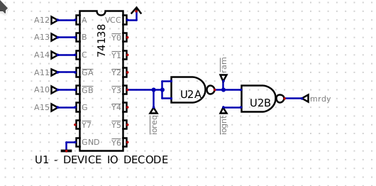
Just two gates, and a 138 decoder IC. A very basic circuit lifted from Brad Rodriguez's Scrounge master design, though due to reasons he lays out in later in his series on the scrounge master, he ended up going another way. For us the circuit is perfect as the AVR solves most of the limits set by the original design, and we don't need the extra latch he uses for clock synchronization. Essentially, the bus decoder waits until it see's a request in the Io-range of 0xB000 to 0xB3FF. Once it is triggered it sends a signal to the two gate request/grant circuit which will send the output (mrdy) to a low state. This holds the CPU to the point in time right before it's data latch. The AVR controls state of /iogrant and holds it high unless it is sending a 'grant' signal. Once the data is either read from, or written to the bus the AVR sends /iogrant low which sends the output (mrdy) high. A high signal on the mrdy signal lets the CPU pick up where it left of and it latches the data as 'E' falls. This set up has three pitfalls.
- The CPU can not be held off longer than 6uS per its data sheet, it's registers are dynamic and need to be refreshed.
- The AVR has to control the low state of /iogrant using a timing delay generated by no-ops to prevent mrdy from 'bouncing low' before the request cycle has completed.
- the AVR can not 'be in two places at once' - that is; it can not control the timing on the grant signal AND clear the bus of the data port at the same time.
We solve these problems thusly: First every operation has to be kept to 6uS -- this is 100% achievable using careful coding - even with C, however every opportunity to quit to the exit of the current poling loop must be taken. Second, we carefully time the delay using an analog scope to properly calculate and test the exact delay, through testing this is approximately 500nS at 2 MHz and 1us at 1 Mhz. NOTE: this delay is not a part of the 6uS limitation on MRDY, in fact once we send /iogrant, MRDY's low state ends and any delay that happens only has to clear the end of the data latch and the next data latch (this is almost another 500nS which is plenty of time. Third, since we have to use the AVR to manage the timing delay we can use a bus transceiver to clear the data port of the bus by controlling it's enable input with /ioreq. Essentially as soon as the delay is over we are already off the bus, and we can start the next poling loop shortly, since MRDY is managing the timing of the CPU latch phase it's relatively unimportant that the poling loop has not started just yet but through testing I've verified the AVR can pole fast enough to hit the top of the loop multiple times within a single E strobe.
Bus Master:
In addition to sharing the bus as a peripheral the AVR can also write to the system ram as a bus master. It does this (for now) using a pair of address latches to hold the memory address while it strobes the data into the memory. Running at 16Mhz, we still need to slow the memory strobes down in order for the data to properly latch into the 55ns memory module, so this process happens relatively quickly - even though it has to be latched. We perform this operation at boot up to accomplish this:
- AVR sets the pins on the micro controller, in order to get it into a working state.
- AVR sends /reset & /halt on the 63C09 to low. This effectively sends the buses on the CPU to high-Z.
- AVR starts timer 2 sending a 4 or 8 Mhz Square wave on pin 21, this is hooked to the clock input on the 63C09.
- AVR waits 10ms for the system state to stabilize.
- UART Starts on the AVR at 115200 baud
- AVR flips some of its 'input' pins to 'outputs' so it can control some of the signals, primarily those that control the bus transceiver.
- AVR strobes the data into the ram chip using 3 bus writes, it clocks the two latches on the first 2, and then clocks the /wr line on the ram chip. Currently this data is stored in program memory on the AVR using a large array, however there's plans to use SD as a means to load the ram chip as well.
- AVR reverses the signals into the 'peripheral' state and releases /halt and /reset,
- CPU looks at the reset vector after a number of dead clock cycles and jumps to that location, having been previously staged by the AVR the system is bootstrapped and running from this point.
Banking the ram chip:
Since we do need signals to control the ram chip's inputs during regular operations (and the signals generated by the CPU aren't quite enough) we build a small circuit to generate the needed signals:
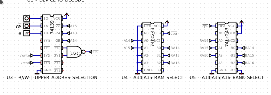
The 74HC139 in the design is used to create both the /read and /write signals for the ram chip, as well as control the two 4 bit bus transceivers which handle the top 3 address bits on the ram chip. In hindsight I totally could have used a 2 to 1 MUX here, I think the 4 bit transceivers are technically faster, but by a matter of a few nS. This is definitely something I'd like to test out for the benefit of the reduced chip count. I really do prefer the 139 for making the more 'intel' compatible control signals, you can get faster / cleaner edges with most of a SN74HC00 or some noise resilience with a SN74HC132, but a 139 offers a whole second decoder, which can reduce the chip count in your design, I think its a fair trade off. The output enable is actually logical NOT /ioreq. This is sourced directly from the middle of the request grant circuit. not pictured is a single 74hc125 which helps to drive the various signals to High-Z at the correct time, and inhibit output enable on the main bus transceiver if needed (like in the case of a device request to another part of the open 1k of address space, which the firmware in the AVR has to account for by reading the state of this line in a poling cycle. Also 1 tri-state buffer is wired to send MRDY to a high state during system reset, to assure the CPU does not enter MRDY during memory staging.
Considerations:
As stated previously, I would like to reduce the chip count to get the over all build cost down further. Some avenues I have already discussed like replacing the 243's with a single 2 to 1, 4 bit MUX. Another avenue of testing would be to try to stage the ram using the CPU, instead of latching the data into external latches. one way we could accomplish this is by using the CPU to set the reset vector in the ram (the busses are tied high, so we would only need 1 address line to do this.) And then create a little machine language program that can run within the 8 byte address space of the device address space. a psudo code example might be something like:
- stage 0xFFFE and FFFF with the AVR setting them to 0xB000 during system halt.
- reset the CPU
- CPU reads reset vector at 0xFFFE and 0xFFFF.
- CPU JMP's to 0xB000 - the first address of the AVR
- AVR enter's a special, boot time only iorequest cycle and provides :
- load a register with first byte from rom
- load direct from a to location in ram
- load x with value of a counter from addressed space on AVR which contains a counter of each byte to load wich the AVR decrements each successive read.
- skip if x is zero
- jump to 0xB000 (the next byte is read - code is sort of self modifiying)
- read from a location in the AVR which returns 00, and internally the AVR resets the CPU and clears the stageing state.
This might be possible to test without any system modification, If we can eliminate the latches this frees up two pins on the AVR for Whatever we want (including more address space if that is desired). The disadvantage here is there is no way to verify the data writes to ram, and the AVR looses the ability to be a bus master. I'd be interested to hear feedback on what thoughts are about changing to this style of memroy stageing. Its definately optional as the current set up works, however the two clock lines for the latches , and the latches themselves are useless untill the sytem is again cold reset.
Another consideration is the request / grant circut could be improved to work with falling edge detection. a good place to start might be a pair of j/k falling edge triggered flip flops. They come in a dual package, and could perhapse be wired to generate the same results as the current circuit. The advantage to using a latch, would be to eliminate the required delay calculation for the /iogrant line, this could free up cycles in the AVR and help to push the over all 63C09 system clock even faster, I still need to think about this some more, i'd only like to make the change if I can eleminate a whole package, I don't want to further clutter the board with more chips as the existing layout is already a nightmeare to route.
Conclusion:
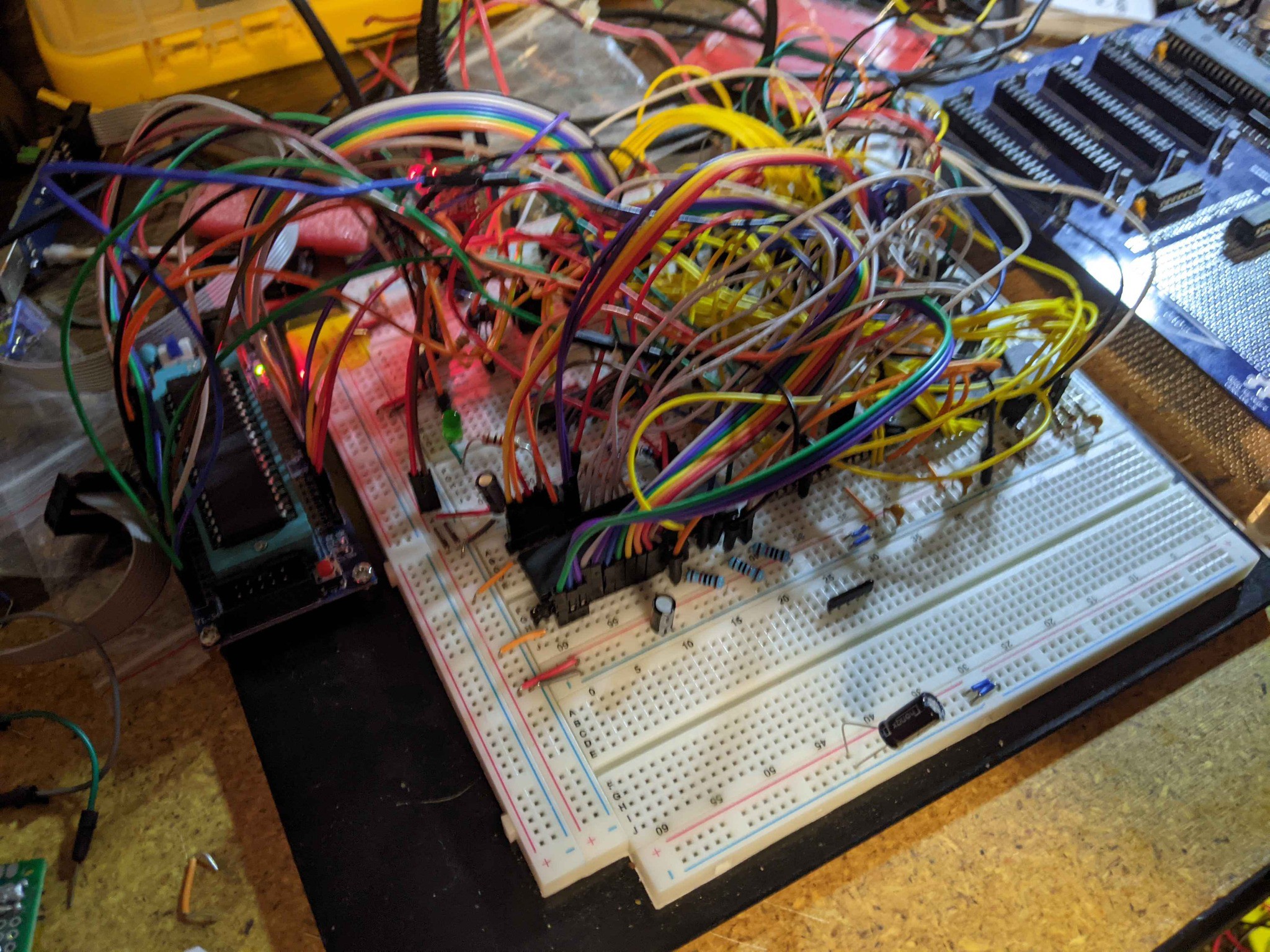
The boards are off to PCBWay, and in manufacture currently. While I wait I have the breadboard prototype to experiement with the firmware. I am hesitent to make any design changes to the nightmere of wires the breadboard has become:
In the meanwhile I want to thank you for taking the time to review my project. I have some schematics loaded into the files section at the top of the project page, and you can review the spreadsheet that outlines the memory map further. I think I made enough space in the memory map that level 1 of OS-9 compatibility should be feasable, though its a long way off if its even possible. The applications for having a uni-paripheral are almost endless, the AVR can interface modern serial protocalls like SPI and I2C as well as provide a buffered UART using the relitively simple 6850 UART protocal (think a 6850 but with a FIFO!). Its a long road ahead but an exciting one!
See you all in a week or two once the prototype is assembled!
Discussions
Become a Hackaday.io Member
Create an account to leave a comment. Already have an account? Log In.