 Viktor Nikolov
Motivation: Why MicroZed?
I'm an electronics enthusiast who got fascinated by FPGA and AMD Xilinx Zynq-7000 System-on-Chip. I found that great development boards exist for Xilinx Zynq-7000, allowing you to explore and play with the platform (for example Zybo Z7). But how do you use Zynq-7000 "in the field" on the final HW device you built? A development board like Zybo Z7 (12 cm x 9 cm) is not very practical for such purposes and is not meant to be used like that.
For Arduinos, ESP and other micro-controllers, you can choose from an extensive offering of small-factor breakout boards, which you insert or solder into your own HW. Unfortunately, I discovered that in the world of Xilinx Zynq-7000, the offering of non-development boards is limited.
After doing some research, I decided to use Avnet MicroZed in a hobby project of mine. This System-on-Module was introduced into the market back in 2013. Avnet did the last revision at the end of 2020, so I hope MicroZed will still be available for some time. It's a relatively compact board (10 cm x 6 cm), comes with very detailed documentation, and one of its perks is the Ethernet interface (important for my project). There are two versions of the MicroZed. One is using Xilinx Zynq-7010 SoC, and the other uses Zynq-7020 SoC.
Please note that to program the MicroZed board, you will need a JTAG programming cable (I recommend Digilent JTAG-HS3 Programming Cable).
Banks, voltages and power-up sequence
Another difference from the microcontroller breakout boards is that you can't just plug the MicroZed into your PCB and start using its I/O pins. The concept of MicroZed SoM is that you plug it into a "carrier card" which provides: 1) circuitry necessary for the MicroZed I/O pins to function as expected; 2) peripherals to be connected to the MicroZed (i.e., the circuitry because of which you created the project in the first place)
Your carrier card has to provide power to the MicroZed I/O pins. This is to give you the flexibility to choose a voltage level for I/O pins to operate on. I/O pins of Xilinx Zynq-7000 are organized into "banks". Banks are identified by numbers. MicroZed provides 53 pins from the Bank 34 and 53 pins from the Bank 35. The more expensive version using the Zynq-7020 chip provides an additional 16 pins from the Bank 13.
Each pin bank has its own power rail (designated as VCCIO). VCCIO can provide 1.8 V, 2.5 V or 3.3 V. Selecting VCCIO voltage is a crucial design choice. For basic low-speed I/O, 3.3 V is OK (e.g., connecting components to the Zynq by SPI). But if you need more advanced stuff (e.g., using fast differential signals), you must select 1.8 V or 2.5 V because Zynq-7000 can't do differential signals on 3.3 V (you can check this Xilinx support article for details).
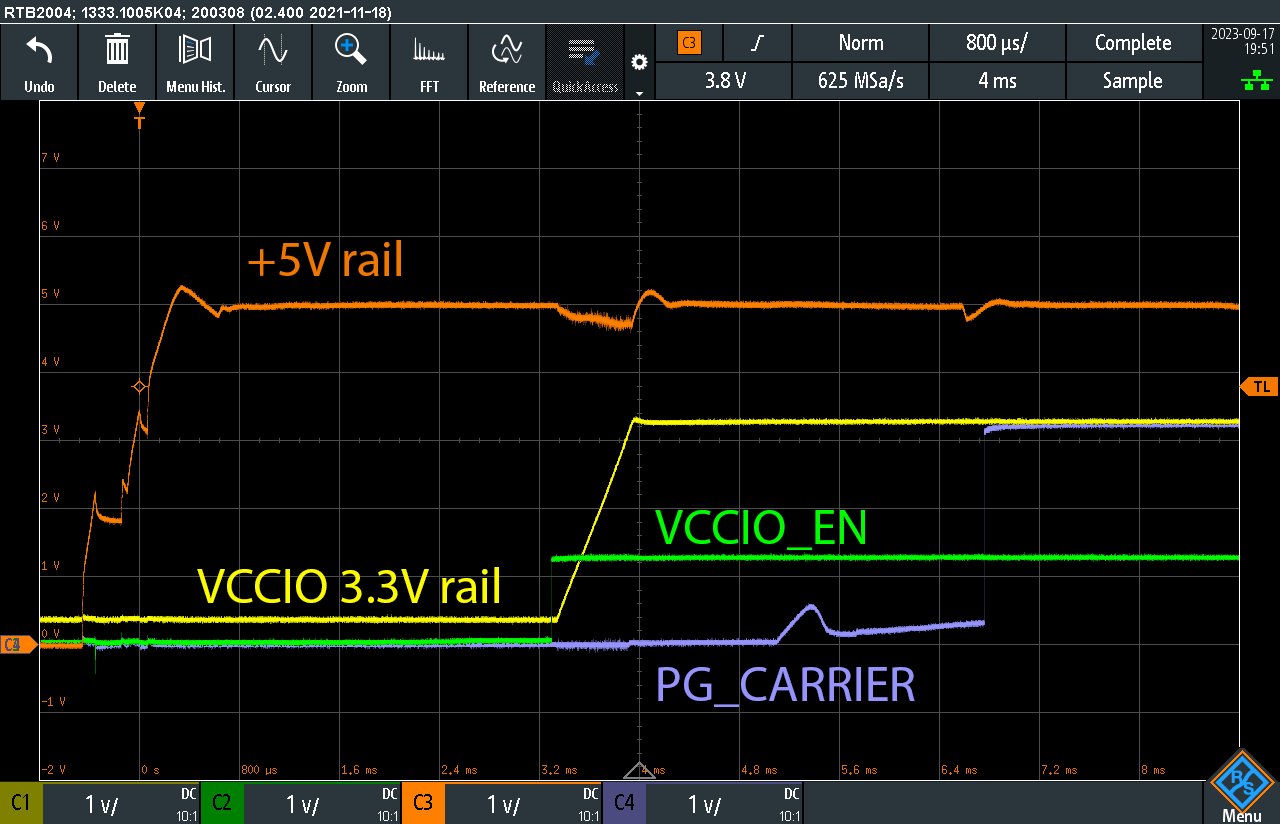
In addition, you have to ensure proper power-up sequence. First, the power rails on the MicroZed start. When done, the signal VCCIO_EN provided from the MicroZed to the carrier card goes high. Only then can the VCCIO rails for the Banks 53/54/13 start. When the VCCIO voltage stabilizes, the carrier card sets the "power good on carrier" signal (PG_CARRIER) high, which goes back to the MicroZed.
Basic design decisions
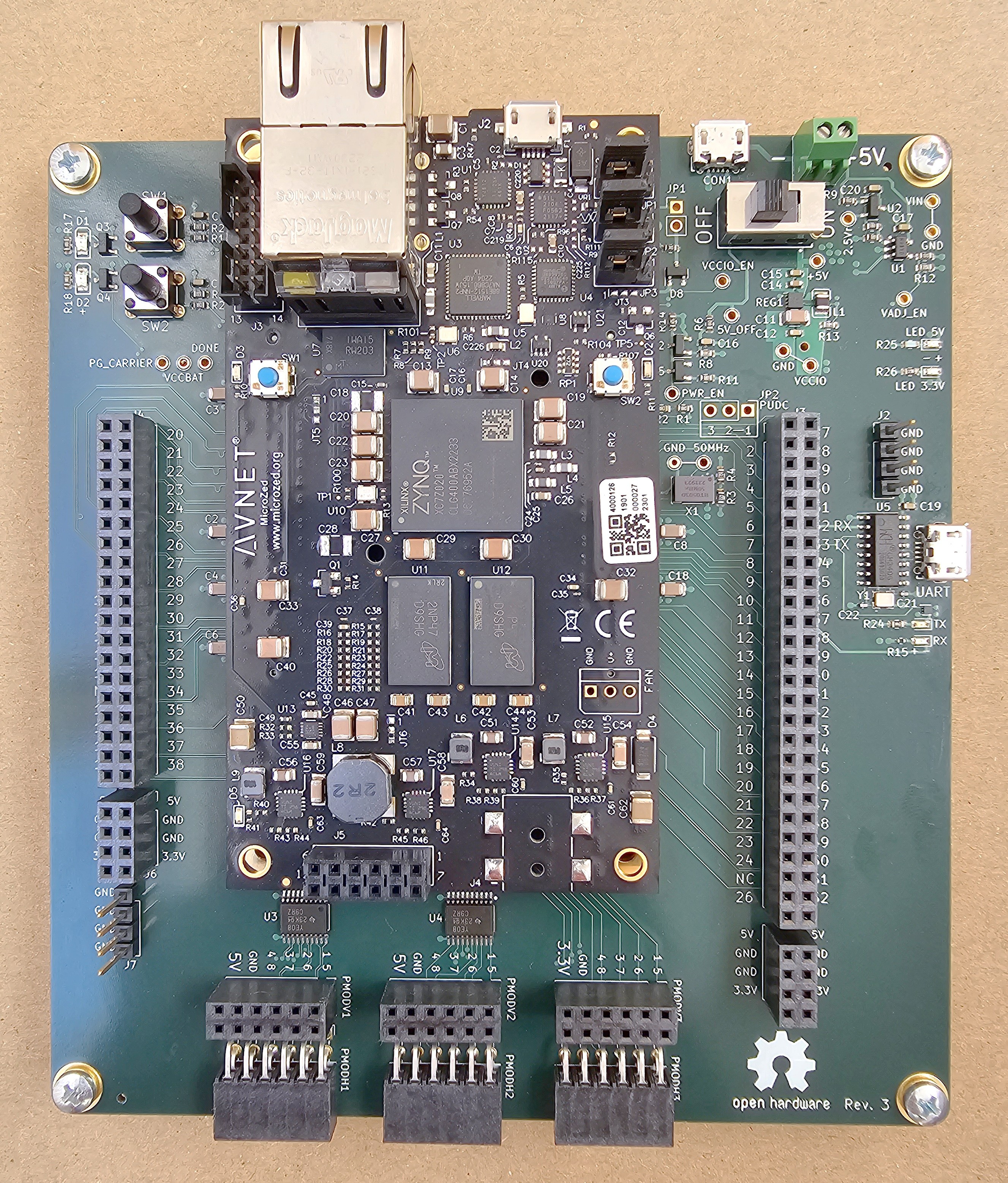
So, I knew I wanted to use the MicroZed in a project, and thanks to its detailed documentation, I became aware of the complexities explained in the previous chapter. Therefore, I decided to build a development carrier card as a "teaching case" and use the gained experience later when designing a future project's PCB, which will "carry" the MicroZed.
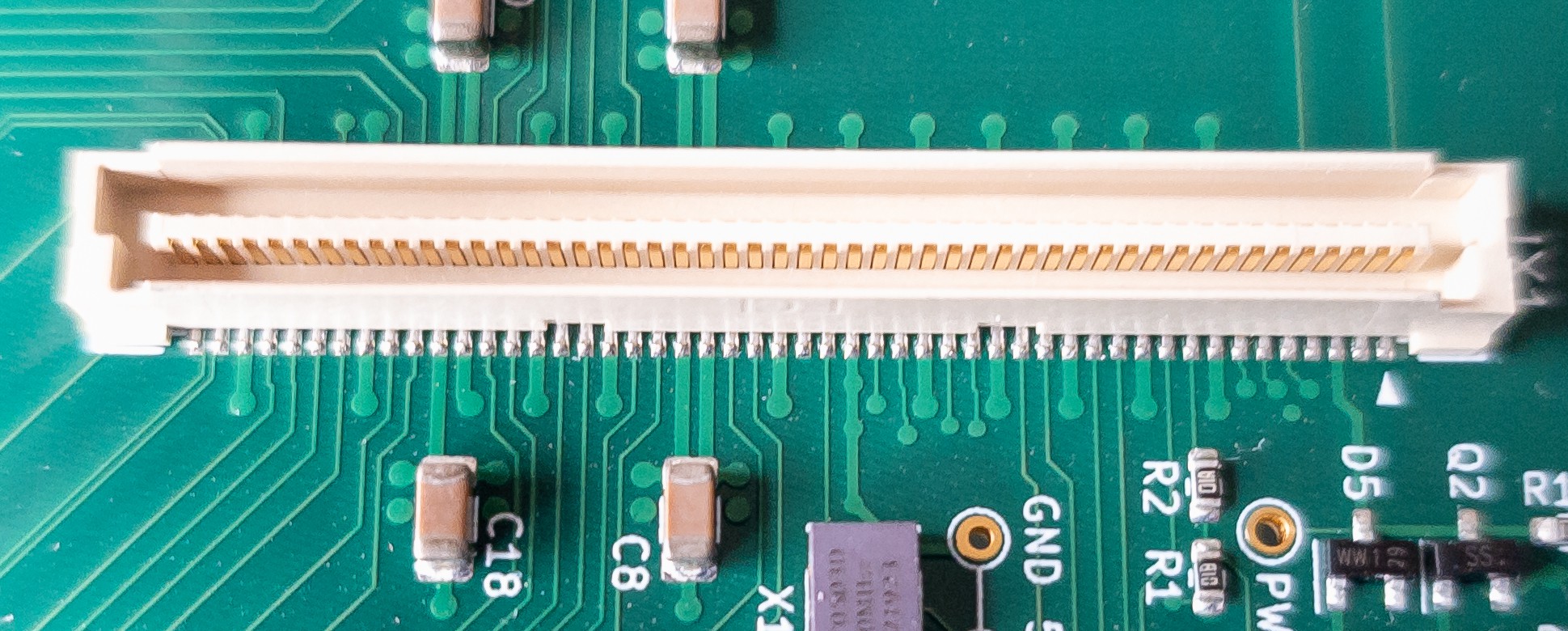
I chose to design the board from the beginning with the intention of having it professionally assembled at a factory. My soldering skills do have limits, and I knew there would be tiny components difficult to solder manually (I don't have a reflow oven nor experience using a hot plate). For example, the two 100-pin BergStak connectors between the MicroZed and the carrier card have soldering pads 0.3 mm wide and 0.8 mm apart, i.e., just 0.5 mm of space between them.
PCB assembly suppliers typically have their parts libraries, and you should strive to use the parts available in the supplier's library as much as possible.
I have experience with JLCPCB, so my selection of parts for the project (done in August 2023) was very much dictated by parts available in the JLCPCB Assembly Parts Library. Please see the Wiki in the project's GitHub repository for details on specifying JLCPCB parts in the design and ordering the manufacturing. (I'm not affiliated with JLCPCB in any way, I'm just using them as my supplier.)
I decided to power all pin banks with VCCIO 3.3 V because my project doesn't require the handling of high-speed differential signals. Nevertheless, the board can be easily converted to VCCIO 1.8 V by simply replacing 3.3 V regulator REG1 TPS62082 with 1.8 V version TPS62081. (Oscillator X1 and UART-to-USB IC U5 will not work on VCCO 1.8 V, but these two components are not critical and can be omitted from PCB assembly.)
Inspired by this great video by Rick Hartley about grounding and signal integrity, I choose to have a 6-layer PCB with layers used as follows:
- front layer: signal
- 1st inner layer: GND
- 2nd inner layer: VCCIO 3.3 V rail
- 3rd inner layer: signal and GND
- 4th inner layer: GND
- back layer: signal and 5 V rail
Please note that the manufacture of my carrier card is not exactly cheap. Production of the final revision of the card by JLCPCB (2 assembled boards + 3 spare PCBs) cost me $194 + shipping costs. (However, you can save $33 if you exclude the 50 MHz oscillator X1 from the assembly.)
Powering the card
The default way to power the carrier card is the micro-USB connector CON1, which has no other function but a 5 V power supply. Connecting power to CON1 (or screw terminal J1) is mandatory for the MicroZed and the card to operate. When also the micro-USB connector on the MicroZed is connected to a computer, the two micro-USB connectors contribute to the current delivery for both MicroZed and the card.
Alternatively, the card can be powered from a lab power supply via screw terminal J1. WARNING: There is no polarity protection on the terminal J1. I didn't want a voltage drop of a protective diode. In the case of wrong polarity, components on the carrier card will be damaged, but the MicroZed will be safe. The MicroZed has a protective Schottky diode D9 on its 5 V input.
I put a power switch on the card. When the card is connected to the power and the switch is off, the PWR_ENABLE signal of MicroZed is driven low, and the MicroZed is shut down.
VCCIO 3.3 V power rail
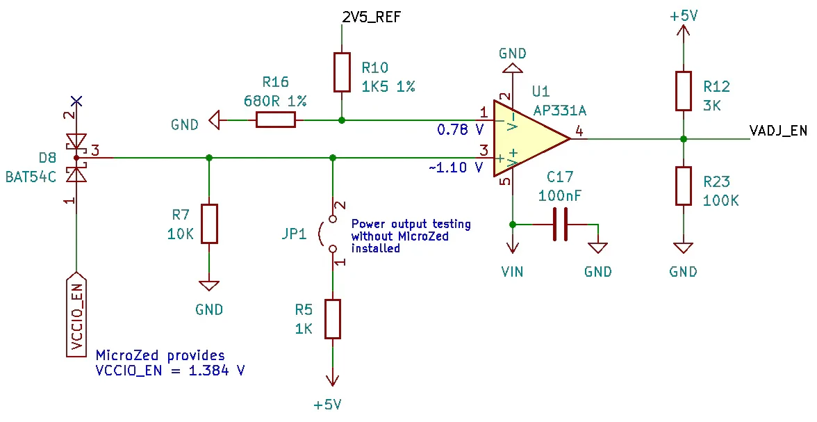
As explained previously, VCCIO can be powered up only after signal VCCIO_EN from the MicroZed to the carrier card goes high. I measured that the MicroZed sets VCCIO_EN to 1.38 V as "high".
The circuitry on the following image utilizes a comparator to generate a 4.85 V signal VADJ_EN when VCCIO_EN goes high. VADJ_EN is then used to enable the output of the VCCIO 3.3 V regulator. To test the VCCIO power rail without the MicroZed attached, the jumper JP1 can be shorted. The diode D8 protects the MicroZed in case JP1 is shorted by mistake while the MicroZed is attached to the carrier card.
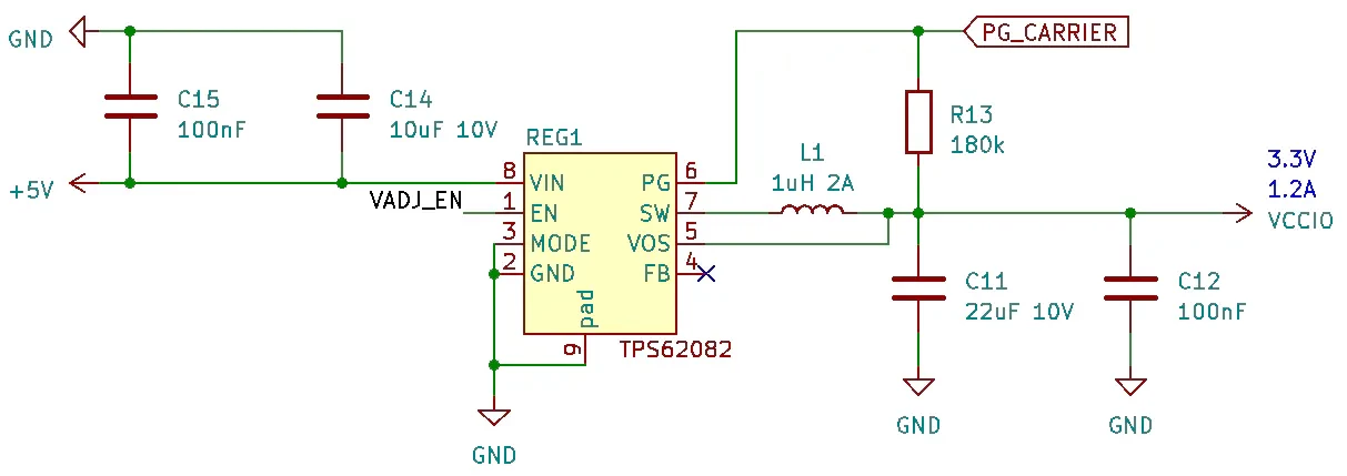
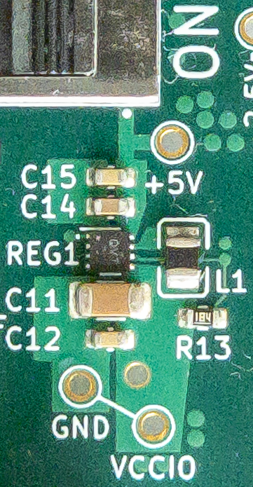
I selected the Texas Instruments TPS62082 step-down converter for the VCCIO rail. I simply followed the TPS62082 datasheet for both the circuit and PCB design.
I, of course, measured the circuit to ensure it worked as expected. The following scope screenshot shows the power-up sequence in the setup when a lab power supply is connected to the screw terminal J1 and is switched on, then the power switch on the carrier card is cycled from the"off" to the"on" position.
I/O pins and other connectors
A development board is supposed to have LEDs, buttons and a lot of pins, right? No problem. The carrier card I present here has 106 digital I/O pins. The pins are exposed on two big female headers, J3 and J4, and on three PMOD headers. Please see the pinout specification in the Wiki of the project's GitHub repository for details. There are two LEDs and two buttons too.
In my projects, I often want to interface with components running on 5 V logic. I, therefore, put two TXB0108 8-bit Bidirectional Voltage-Level Shifters between the MicroZed pins and two PMOD headers.
5 V, 3.3 V and GND for powering external components connected to the card are exposed on two female headers, J5 and J7.4-pin headers J2 and J7 provide ground. I soldered male headers on J2 and J7 and am using them to connect ground leads of scope probes.
UART to USB connection
In my project, I often use UART to output debug data directly from the FPGA Programmable Logic using AXI UART Lite IP. To make it easier, I put USB to serial conversion chip CH340G on the card accessible via the UART Micro-USB connector (this connector doesn't provide any power to the board, just a USB connection). Credit for this part of the board's circuit goes to the SparkFun because I replicated the SparkFun Serial Basic Breakout circuit on the carrier card.
My experience is that no driver installation is needed on Windows and Ubuntu to connect the computer to the CH340 IC. The serial port just "appears" in the operating system. If you face a missing driver problem, download the CH340 IC driver from the CH340 IC manufacturer.
WARNING for Ubuntu: On Ubuntu 22.04.1 (and other versions too) a braille display driver is in conflict with the CH340 USB serial (see discussion here). The issue is resolved by uninstalling BRLTTY by the command sudo apt remove brltty.
To use the UART to USB connection in the Programmable Logic of the FPGA, you need to place an AXI UART Lite IP in the Vivado diagram and connect its TX signal to the Zynq pin U20 (named J3_33_UART_TX in the master constraints file available in project's GitHub repository). The RX signal of the UART Lite must go to Zynq pin T20 (named J3_32_UART_RX in the master.xdc file).
I wrote a simple Verilog module write_to_uart, which connects to AXI UART Lite IP via AXI and exposes a simple interface for "printing" strings up to 16 characters long. See the board demo project for an example of use.
Of course, also Zynq Processing System ARM cores or a MicroBlaze processor core can use the carrier card's UART to USB connection.In the case of Zynq PS, enable the UART0 in the ZYNQ7 Processing System configuration and set its IO to EMIO. UART0_TX/RX signals will appear on the PS IP; connect them to the Zynq pins U20/T20. In the application code, use UART by means of the xuartps library. In the case of MicroBlaze, connect the AXI UART Lite IP to the MicroBlaze via the AXI Interconnect IP, and in Vitis select the UART Lite IP instance for stdin/stdout in the Board Support Package Settings.
50 MHz oscillator
A precise 50 MHz oscillator is connected to the Zynq pin N18 (IO_L13P_T2_MRCC_34). The motivation for having this oscillator is to test external clock input into the FPGA Programmable Logic.
The oscillator can also be used as a clock input for the FPGA Programmable Logic testing without the Zynq Processing System running. The Zynq PS clock signal FCLK_CLK0 outputs the 100 MHz clock only when an application runs on the PS ARM cores. On the other hand, the carrier card's 50 MHz oscillator runs always.
Nevertheless, the oscillator can be removed from the production files to save cost.
Demo app
I provided a demonstration HW design and SW code in the project's GitHub repository. I used Vivado and Vitis of version 2023.1. To run the demo on the carrier card: Open the MicroZed 7010 workspace or MicroZed 7020 workspace in Vitis 2023.1. Run Build All. Program Device and then run the board_demo application.
The demo uses a simple HW design and a standalone bare-metal app running on the Zynq ARM core.
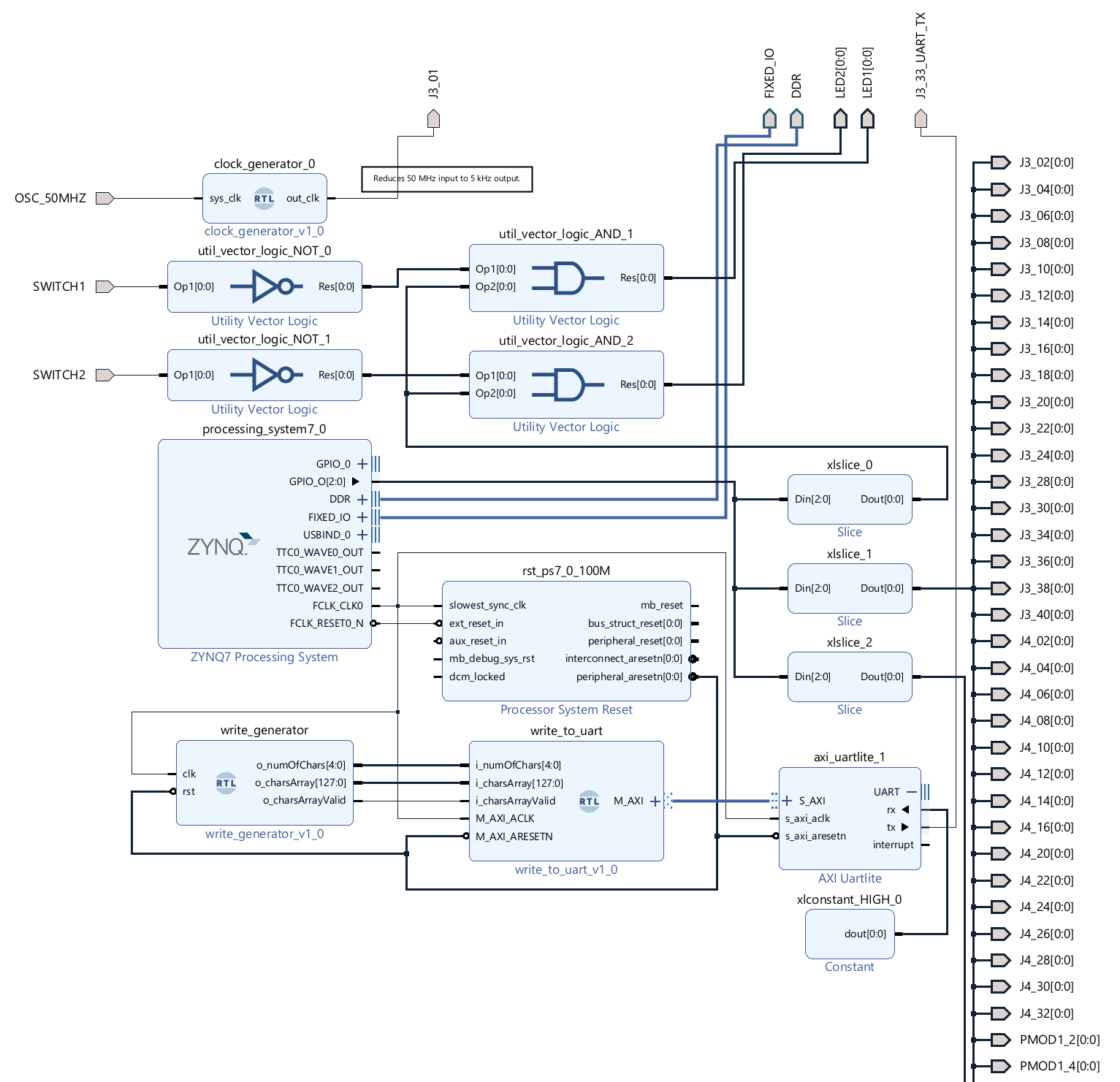
Three EMIO GPIO pins are exposed from the ZYNQ Processing System. They are then sliced into three separate signals.
The first signal drives the card's LEDs. Activation of a switch drives an LED low despite the GPIO signal being high.
The second GPIO signal is connected to ports with even pin numbers. The third GPIO signal drives ports with odd pin numbers.
An instance of a clock_generator module descales input 50 MHz signal from the oscillator X1 by factor 10, 000 on the card's pin J3_01.
Sample UART serial output is generated purely by the Programmable Logic on the FPGA. The module write_generator produces a series of strings containing increasing numbers from 00000 to 16383. The helper module write_to_uart then sends the string to the AXI UART Lite IP via the AXI bus.
The Processing System application board_demo.cpp is pretty simple. It initializes the GPIO driver and then changes the state of the three GPIO signals in an infinite loop to generate square wave signals of different frequencies.
The demo app does the following:
- The carrier card's LED1 and LED2 blink with a 2.5 Hz frequency.
- The card's SWITCH1 disables blinking of LED1. SWITCH2 disables LED2.
- Testing serial output (speed 9600 baud) is provided on the UART Micro-USB connector as an increasing series of numbers (25 lines per second).
- The card's pin J3_1 provides a square wave signal of frequency 5 kHz.
- Other pins with odd pin numbers on J3, J4 and PMODs provide the square wave signal of frequency 166.6 Hz. Pins with even pin numbers on J3, J4 and PMODs provide the square wave signal of frequency 80.6 Hz.
Final thoughts
Can an electronics enthusiast use the MicroZed SoM? Yes, he or she can. Even a not-very-advanced enthusiast like myself.
I hope the information summarized in this article and the resources I published on the GitHub repository will help you in your journey.