 macafeeje
Obligatory danger warning; there are several high potentials within an oscilloscope which you should become familiar with before opening any such device. Proceed with caution.
Original Fault Finding;
The list of faults when I first received my particular PM3310 was extensive. Most obviously there was no trace, only a single dot. I did not get round to investigating this fault immediately, as the scope would not pass it's boot check and it seemed logical to pursue this particular issue before looking at anything else. Once the scope was repaired to the point of passing a boot check, the lack of any X deflection became my next task.
I will limit my notes on the repairs to the board A20, the final amplifier, and in case it's useful...
- PCB under V2023 found to be discoloured with heat, tested to be defective. (V2007, 2016 and 2032 replaced as a precaution)
- V2038 tested to be defective
- D2023 (oq0017) signal in from D2021 found to be good, no signal at the output, suspect D2023
The scope was tested after replacing the defective transistors, however there remained no trace to be had.
It is not known whether the chip (D2023 - oq0017) failed first, causing the transistor to overheat and fail, or if the failed transistors (current source above pins 12/13 and/or constant current source at pin 9) ultimately lead to the demise of our X amplifier chip. From my research there have been a few X amplifier chips failed on this model scope, and whilst I could not speak to their exact means of failure, it does appear to be a common fault.
Other faults on A20;
- R2081 insulation broken, "sparking" from +125 to GND or +12 nearby traces (occurred after the above fault finding).
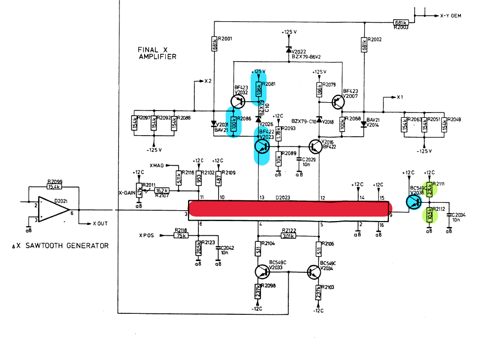
This excerpt from the PM3310 service manual (edited for context) shows the final X amplifier arrangement. A ramp signal is generated and buffered by the op-amp D2021 before the chip on pin 3. The X POS line to pin 6 is the left/right position of the trace, as controlled by the X POSITION dial on the front bezel. The gain is controlled as a product of X-GAIN, x1 gain adjustment, and X MAG, the x2.5 magnification dial. Pin 9 is a constant current source for internal chip functions.
Whilst the engineers creating the service manual left out the inner workings of oq0017, some though was given to its layout as pictured here. There is something to be inferred by the above and below symmetries from pin 13 to pin 4 and from pin 12 to pin 5. It could be reasonably assumed that a differential current between these two pairs would cause the X1 and X2 plate deflection voltages to vary, guiding the CRT trace from left to right with the ramp signal.

Early Attempt;
I include my earliest attempt at restoring an X trace here, as it is very simple to implement and could be done easily with a few minor components. The x2.5 magnification function will be lost.
I was not at all familiar with the pure "analogue magic" that was to come, and so as I started my research into a solution regarding the peculiarities of a variable gain difference amplifier I of course came across the long tailed differential pair. The current source and sink above and below pins 12/13 and 4/5 seemed to fit with this topology.
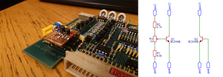
Q1 and Q2 form the differential pair, that is the difference between the X ramp signal and the left to right position as set on the front X POSITION control. Ideally both transistors should be matched, and to reduce the effects of thermal drift, both should be thermally bonded to each other (most simply with the use of a zip-tie).
R1, 2 & 3 form a potential divider as a crude method of reducing the gain of the ramp signal. To set the trace width, R3 allows for a trimmable final gain.
The PM3207;
I stuck with the above arrangement whilst repairing the seemingly increasing number of faults with my scope. Later, I did find a repair log by (I think) Markus Dropmann in 2016 (google "Reparaturbericht digitales Speicher-Oszilloskop Philips PM3311" or try here). Being a resourceful chap, he found the internal workings of our chip, the oq0017, detailed in the PM3207 service manual. The answers to all our questions at last!

Unfortunately it is a simplified drawing, missing at least one particular section to be looked at later. We can, however, note the Darlington input stage mentioned in our service manual (as formed by V15, 16, 17 & 18).
A brief aside, the PM3207 uses our chip in a different way to the PM3310. The sections above the current sources CS1 and CS2 can be omitted, as cross referencing our PM3310 schematic, they serve no purpose for us.
That simply leaves the transistor arrangement at the very top, V1 to V4. More analogue magic; a Gilbert cell multiplier. I have come to imagining the Gilbert cell (a four input signal multiplier) as two long-tailed differential pairs cross coupled with one another, sourced by a third differential pair. This is the key to magnifying our normal trace with the differential signal between pins 10 and 11. Our friend Markus was already on it, recognising the topology from various frequency mixer designs. He went so far as to bench test a prototype, an oq0017 replacement of his own device, however he happened upon a replacement chip before he could test his in the scope proper. I believe it wouldn't have worked exactly as designed, as I tried the above schematic in a simulator and on a breadboard on top of the scope to no avail.
The Missing Buffer Section;
From the description provided in the service manual of the oq0017, we are possibly missing the "buffer stage". When trying the circuit in a simulator, I found that the transistors in the Gilbert cell would no longer conduct from the plate deflection sources (pins 12 & 13) as the voltage at the transistors base (pins 10 and 11) was greater than the voltage above the cell.
First I tried lowering the voltage from pins 10 and 11 with a potential divider arrangement. This worked to a degree, but the trace displayed on the CRT was very non-linear. This is, I suspect, because of the relatively low impedance of the Gilbert cell versus the divider networks. The solution was to keep the voltage constant at the Gilbert cell with a buffer stage. How the oq0017 does this internally I do not know, but I suspect it to be a cleverer arrangement than mine.
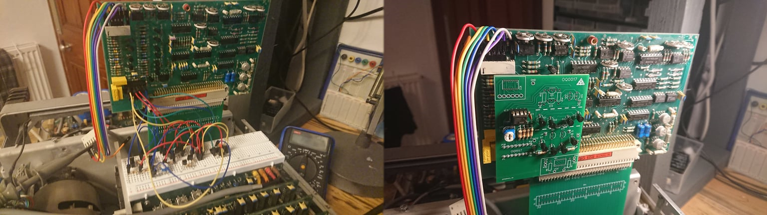
The breadboard prototype I was experimenting with grew to be quite unstable, owing to various poor connections and the stray inductance of many jumpers. I designed and sent off for a development board, one which would allow the test of several different configurations whilst being plugged directly into board A20.
In short summary of my various tests, I found that an op-amp buffer was less stable and less linear than the NPN/PNP transistor buffer, and that omitting the biasing stage would cause all sorts of weirdness. I also determined the biasing point could be set to a common 5v constant voltage reference (the biasing point must be above the max voltage at pin 3, the input to the Darlington stage (approx 3v), and below the potential divider voltage at the output of the buffer stages minus the voltage drop through the Gilbert cell). The end result was an all discrete transistor arrangement, which restored the full functionality of oq0017 including the x2.5 magnification.

NB: omit R8 and R9
This design can be implemented, as I did initially, with discrete components. I used BC549B and BC559C transistors that I had to hand, and v_bias was set using a typical LM7805 5v voltage regulator and some capacitors.
Its main disadvantage is that without transistors with matched thermal characteristics, it remained susceptible to drift.
Final Design;
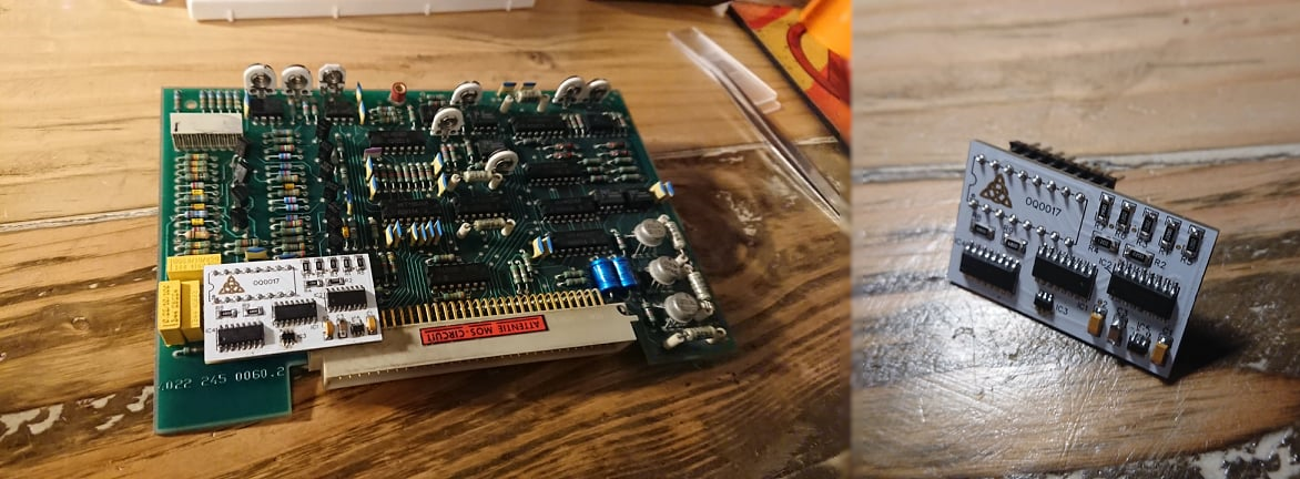
The final schematic above uses transistor arrays in a SOT-16 package, so as to remain hand solder-able whilst keeping the form factor to a minimum. Having the 4 transistors in one package for the Darlington input stage and the Gilbert cell should mitigate some of the issues with thermal drift. Even though these are not matched transistors, they are on the same die and so their properties varying with temperature should do so together at a similar rate.
Matched transistor arrays are out there, but after building my replacement I found the thermal drift to be much better than the discrete BJT versions and only a tiny margin worse than an original oq0017 (I should note, maybe, at this point that I am the proud owner of 2 PM3310 scopes, one of which has an original working x amplifier).
Here you can see the results, on a stylish white PCB with ENIG gold flash (I am nothing if not flashy), however it pains me to say it did not work immediately. After an hour or two of debugging I found than I had read the pinout of IC5 (FMB3904) wrong from the datasheet. Very fortunately, by turning the chip around 180 degrees everything lines up as it should.
With everything working, I soldered it in place and reconnected everything to the A20 board, and unfortunately, it stopped working. The extreme left and right ends of the trace were undergoing a "jittering" motion. I found that by disconnecting the calibration output (the red coax, top centre of board A20) the jittering went away. To cut a long story short, the current draw of the square wave probe calibration output was enough to cause a 50mVpp ripple on the +12C supply rail. Ripple was causing the magnification to vary slightly between each pass of the trace therefore creating a "jittering". In all my design and testing, it occurs to me that I never would have connected the cal signal. I observed the same ripple on the scope with an original oq0017 which tells me that they had a different approach to the buffer section, one less susceptible to common mode noise.
There is an easy fix; by omitting R101 (found directly attached to the CAL socket on the front panel, either by cutting or removing, the current draw and therefore ripple generated by this sub-circuit is removed from the +12C voltage rail and the "jittering" stops. The probe compensation function is not lost, as the 3V square wave can still be utilised, however I believe there was an option for a 6mA square wave calibration function which would no longer work - though I can't say I know what that would be used for anyway. Overall, I deemed this to be an acceptable compromise, even though it voids one of my design requirements to not have to modify the scope in any way. Another option would be to increase the values of the RC low pass filter for the +12C rail (R2119 and C2036), however I am satisfied with this solution.

Overall I am very happy with the time spent on this project, though there were moments where I feared it would never end. At last count there were 18 total faults with my scope, and with this one solved there is only 1 left. But, something to do another day, perhaps.
P.S. If you want one of these you can have one at cost (some assembly required) or if you have any questions/thoughts/comments regarding the oq0017 chip or the PM3310 in general just let me know.
I think these scopes are worth keeping around for a few years yet!