 David Robinson
Counting the GPIOs...
With the intention of using the Raspberry Pico micro controller, I needed to understand how many GPIOs would be required to carry all of the necessary signals:
- 16 X Address Lines
- 8 X Data Lines
- MREQ signal
- WR signal
- RD signal.
This is a total of 27 input / output lines that are required. However, the Pico only has 26 GPIOs.
Some changes had to be made as follows:
- Address line 15 is only needed for addresses greater than 32K, so this line can be ignored
- Address line 14 is high whenever the RAM area of the ZX81 is addressed - it is therefore possible to combine WR, RD and A14 signals to give a composite signal.
External logic was used to perform the combining of WR, RD and A14 as follows:
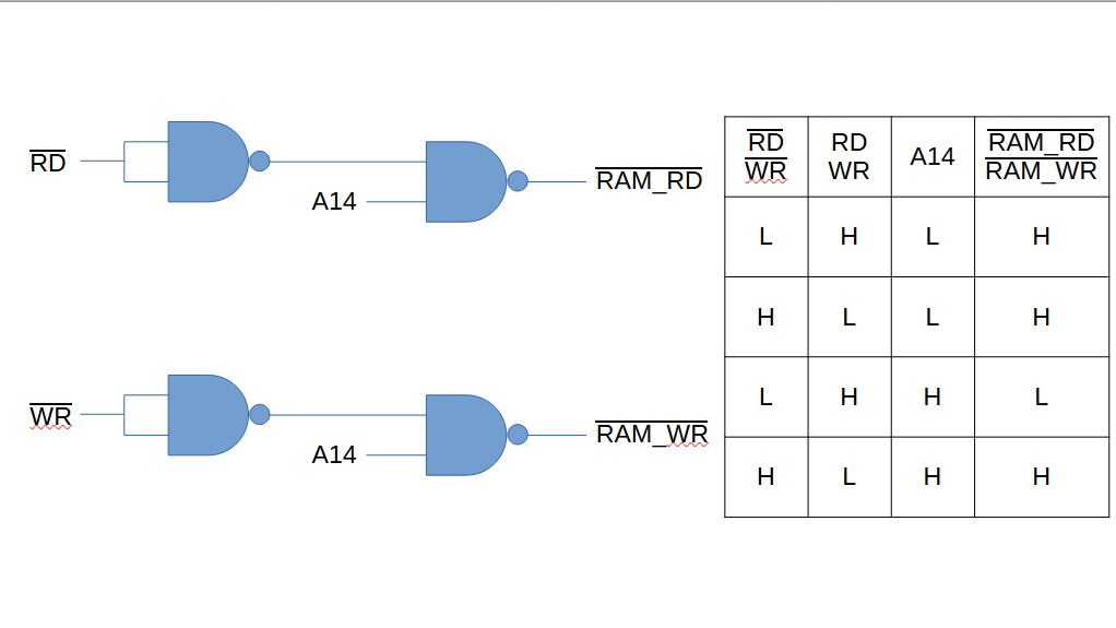
RAM_RD and RAM_WR go low when a read or write is occurring in the RAM area.
So now the GPIO requirements were as follows:
- 14 X Address Lines (A0 to A13)
- 8 X Data Lines (D0 to D7)
- /MREQ signal
- /RAM_WR signal
- /RAM_RD signal.
This is now 25 input / output lines, so there is 1 spare line for other uses.
Voltage Levels...
The ZX81 uses 5V logic, but the Pico requires 3V3 voltage levels. However, it has been stated that the Pico GPIOs are somewhat 5V tolerant - so this was taken to mean forget about voltage shifters and connect the Pico to the ZX81 without any worries - so far this has been a good assumption.
Z80 Timing...
It was important to understand the timing of the Z80 CPU for memory reads and writes. Here is the relevant section from the Z80 chip guide:
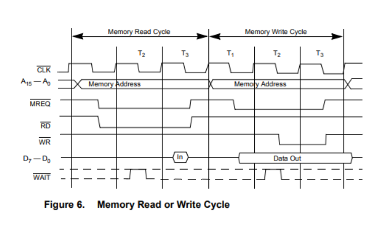
For a memory read, both MREQ and RD go low, at which time the RAM Pack should read the address A0 to A13, locate the correct data byte from memory and place the value on the data bus D0 to D7.
For a memory write, MREQ goes low, then WR goes low after a full clock cycle i.e. there is a delay. The RAM Pack should then read the address A0 to A13 and read the data D0 to D7, then store the data value in memory.
Emulating RAM in the Pico...
To emulate RAM we need to read the address from the address bus and either read or write data from / to the data bus.
So reading address lines A0 to A13 gives is a 14 bit address which needs to be used as an offset into a buffer within the Pico - this is a range of address 0 to 16384, or 0x0000 to 0x3FFF in hexadecimal (remembering that this is the address with A14 high, i.e. an address in the upper 16K address range). Addresses in the Pico are 32 bits, so we'll need to create a memory buffer that sits on a 14 bit boundary i.e.
uint8_t ram[16384] __attribute__((aligned(16384)));
Using 'aligned(16384)' will ensure the memory sits on a boundary with the lower 14 bits of the Pico address being '0'. This will then allow us to add on the address read from the ZX81 address bus to determine the offset into the ram i.e.
Offset into Pico ram buffer = ram + (A0 to A13 from ZX81).
For the data bus, we must either assert the data lines to the ram value, or read the data lines to get the value to store. Also, the data lines must either be outputs or inputs depending on whether a write or read is being performed.
PIO and DMA, no need for a CPU...
Pico includes a hardware section known as Programmable Input/Output - this is essentially an efficient mechanism to read or write data to the GPIOs.
DMA, or Direct Memory Access is another hardware feature of the Pico that allows data to be moved between memory and PIO without the CPU being involved.
Combining PIO and DMA allows for extremely efficient data moving between GPIO and memory without the CPU being involved - this in theory frees the 2 cores of the Pico to perform other tasks.
Putting It All Together...
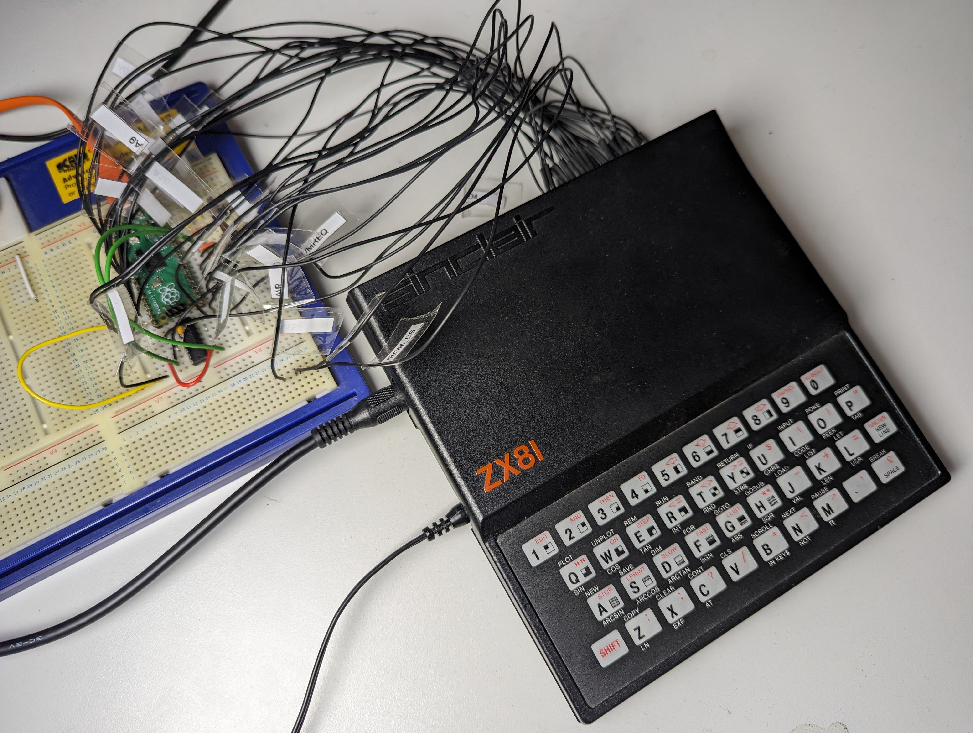
So it's not too tricky to connect everything together...
Wiring Diagram...
         ------
A0     o| PICO |o
A1     o|      |o Connect to 5V for standalone , otherwise leave disconnected for USB power
       o|      |o
A2     o|      |o
A3     o|      |o
A4     o|      |o
A5     o|      |o Button --| Connect normally open button to ground
       o|      |o GND    --|
A6     o|      |o /RAM_RD
A7...
Read more »


 teardownit
 EtchedPixels
 Jac Goudsmit
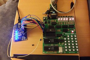
Thanks - I didn't know about the use of the refresh signal. It will be easy to add it as an input to the existing NAND gate along with /RD.