 Tony Robinson
Here is (hopefully) the final memory cell architecture for my processor.
It uses two transistors as a flip-flop to store the state, S. There is also: IN - data in, WE - Write enable, OUT - data out and RE, Read enable.
Write is:
S = (S AND NOT WE) OR (WE AND IN)
(the NOT comes for almost free as it's shared across all 16 memory cells in a register).
Read is:
OUT = S AND RE
Both AND and OR may be implemented with two diodes and a resistor (e.g. http://electronics.stackexchange.com/questions/131860/diode-logic-gates). This is the simplest memory cell I can think of, if you double the write logic you can write to both halves of the flip-flop at the same time which improves speed - but I value simplicity over speed.
So, after fighting http://circuits-cloud.com/ all day (most saves fail and force a reload of the last successful save making progess painfully slow - I'm not using them again), here is the circuit diagram:
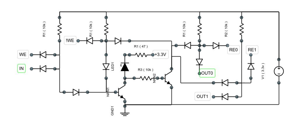
The left hand side does the write, the right hand side does the read (to two buses, 2T 9D is for only one read). Let's say we want to write, then we set WE high and the left AND circuit has the value of IN, where as the next AND circuit is low (as !WE is low). The OR of these two AND circuits is therefore the value of IN. Hence the base of NPN1 is set to IN, if it's high then the transistor conducts and the LED light is lit. R3 sends a low to NPN2 which is then off. When WE is low, !WE is high, so the output of NPN2 is fed back into NPN1 and a bit is stored.
The right hand side does the read and is considerably easier. Both OUT0 and OUT1 are AND functions of the relevant read enable signal (RE0 and RE1 respectively).
If anyone knows of a decent circuit layout for matrix board I really need it.
Discussions
Become a Hackaday.io Member
Create an account to leave a comment. Already have an account? Log In.