 Portland.HODL
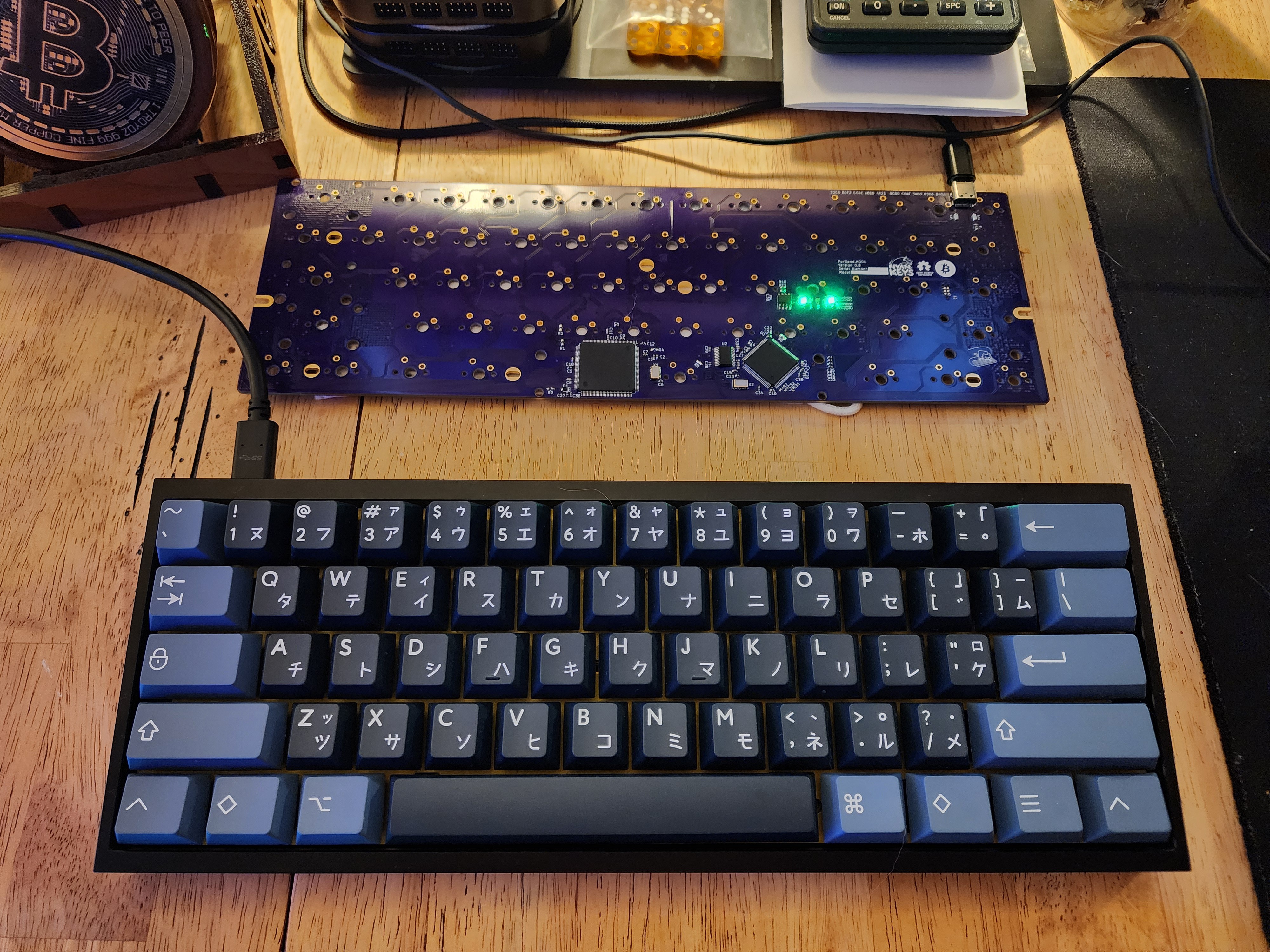
Nyan Keys - Hardware
The purpose of Nyan Keys was to engineer the lowest possible latency mechanical keyboard that would accept any Cherry compatible switches, e.x. Kailh and Gateron.
The hardware inspiration came from the Wooting 60HE and Pok3r 60% mechanical keyboards. Where the performance characteristics of the Wooting were desired but with the freedom to use any off the shelf switches of the Pok3r
Latency 🚀 (The Numbers)
Nyan keys is fast... really fast. Key latency is unmatched at 30µs worst case while the SPI bus between the FPGA and the MCU is running at 12.25Mhz.
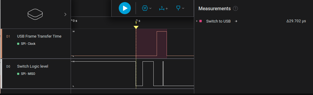
The above is a simple test of when the switch logic level goes low how long until the 'USB Frame Transfer Time' line goes from low->high->low. This is the total time between keypress and the the buffer for the next usb interrupt to be set. This is not the end all be all though. the host still has to interrupt the keyboard at 8000hz to get that data that was just set from from the key press. The bInterval of Nyan Keys is set to 1 at USB2.0 HS, which means 8000hz or .125ms. Lets us assume the worst case scenario where the key is pressed right after the last frame was requested and sent to the host. We would take out 30us latency then add that to the 125us latency of the USB Interrupt transfer to get ~155us. This is 6.5x faster than any usb 2.0 FS based keyboard (The current market) which have an interrupt rate of 1ms and you have to also add in the latency of scanning the matrix. giving Nyan Keys not just the win in the most over engineered solution to a problem that .00001% of people would have, but likely the lowest latency solution available.
Notice how the switch state is sent before the the switch is even done bouncing. This is because you can arm the debounce counter to prevent a state change after the initial press or release of the key.
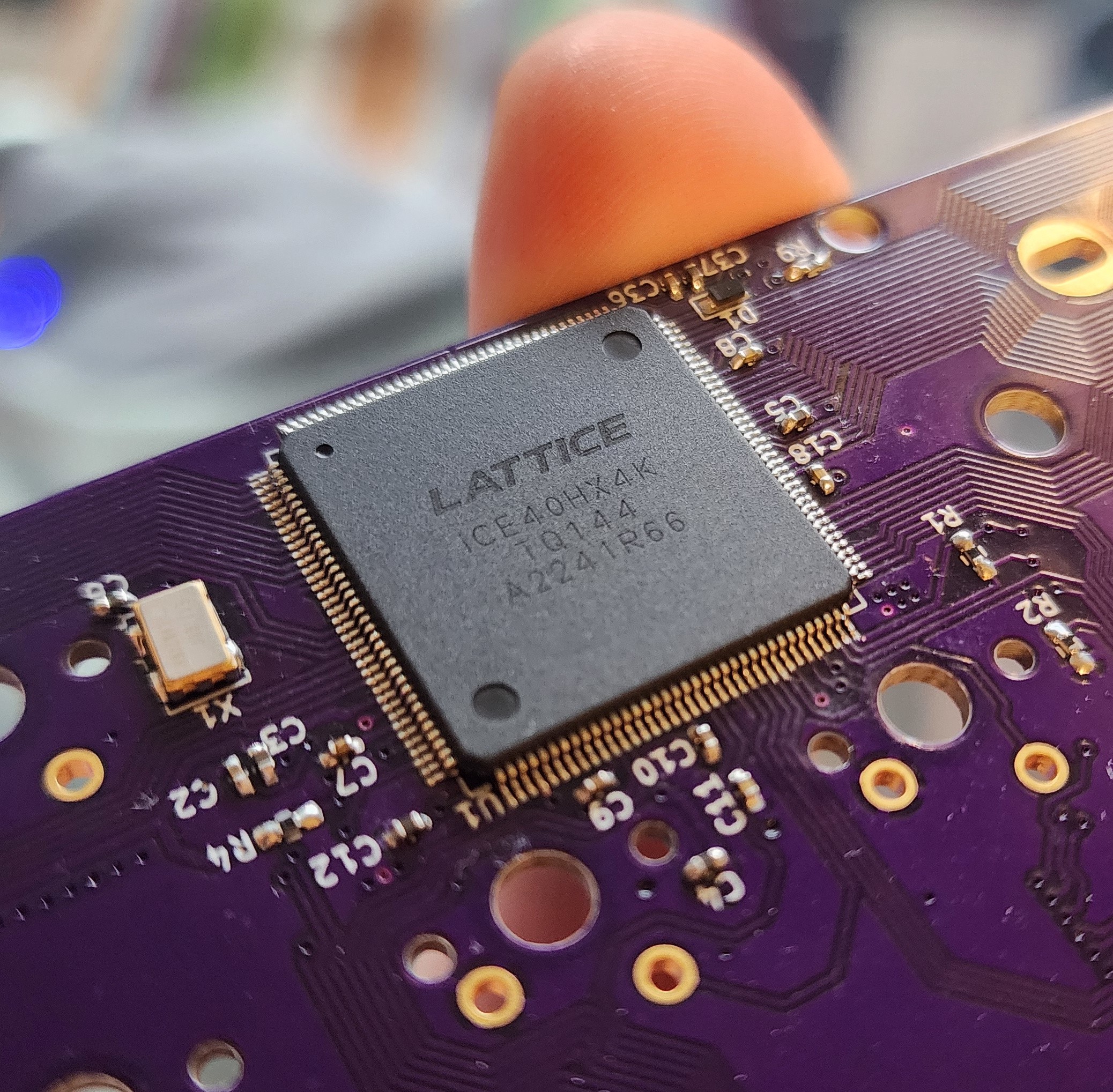
FPGA
The most novel element to Nyan Keys is the use of an FPGA to handle the debouncing logic and serialization of the parallel keys interface. Using an FPGA had the advantage of being able to wire each switch to it's own IO pin, which could be pulled high with the internal pull-up resistors on the Lattice Ice20HX4K IO block. This design greatly increased the routing complexity but at the same time removed any need for additional components such as diodes with each switch.
Using and FPGA allowed for the ability to give each key (switch) it's own core, which consists of an 8 bit timer. The timer is always counting up to the value of 255, once the counter reaches the comparison value the key can change its state and the timer will reset to 0. While the counter is any value that is not 255 the switch state can not be changed. This is the debounce mechanism.
There are 2 primary advantages of the above method for debouncing. The first is that the key press is able to be instantly registered for the press and release as long as the debounce lockout counter has passed. Second it's very area efficient using ~25-30% of an Ice40HX4K for 61 total keys.
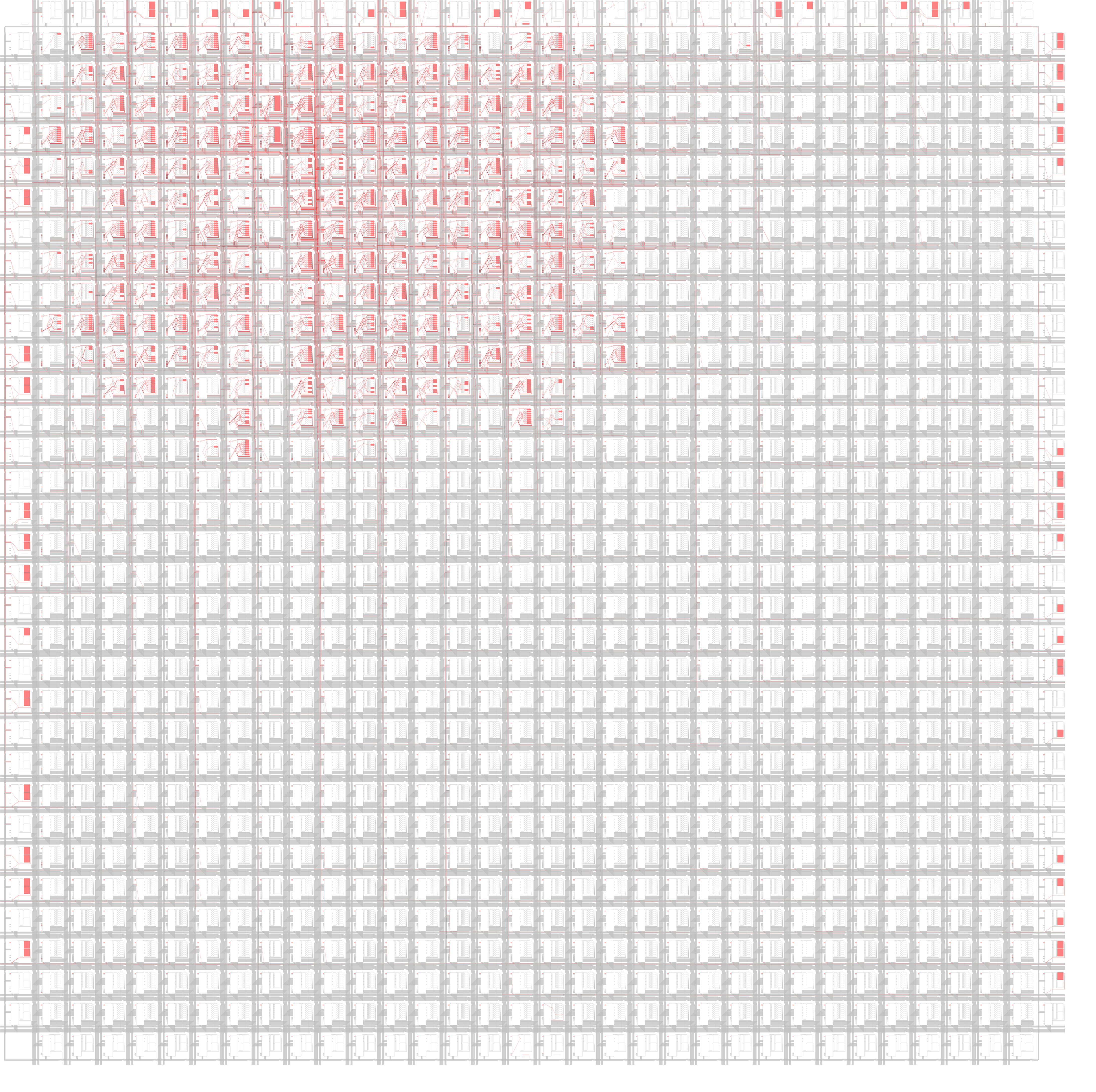
Some of the initial designs were very area inefficient and as such would use a majority of the PLBs of the lattice ICE40 FPGA. This led to the initial versions which had an up AND down counter for the debounce to use more than the available logic blocks on an ICE40HX1K IC. This design was safer from electrical noise and very accidental touches but increased the latency by the time of the counter to even get the switch to change state.
The new revision scrapped all of that an instead just uses an UP counter as such the new logic just uses NUM_KEYS * COUNTER_REG_WIDTH registers and the total area used was reduced by nearly 75% given the same width debounce counters. This can be seen below in the .PNG showing the various elements of the PLB that are used once the verilog is synthesized and routed. This new approach also removed the need to synthesize subtractors and replaced it with much simpler comparison logic.
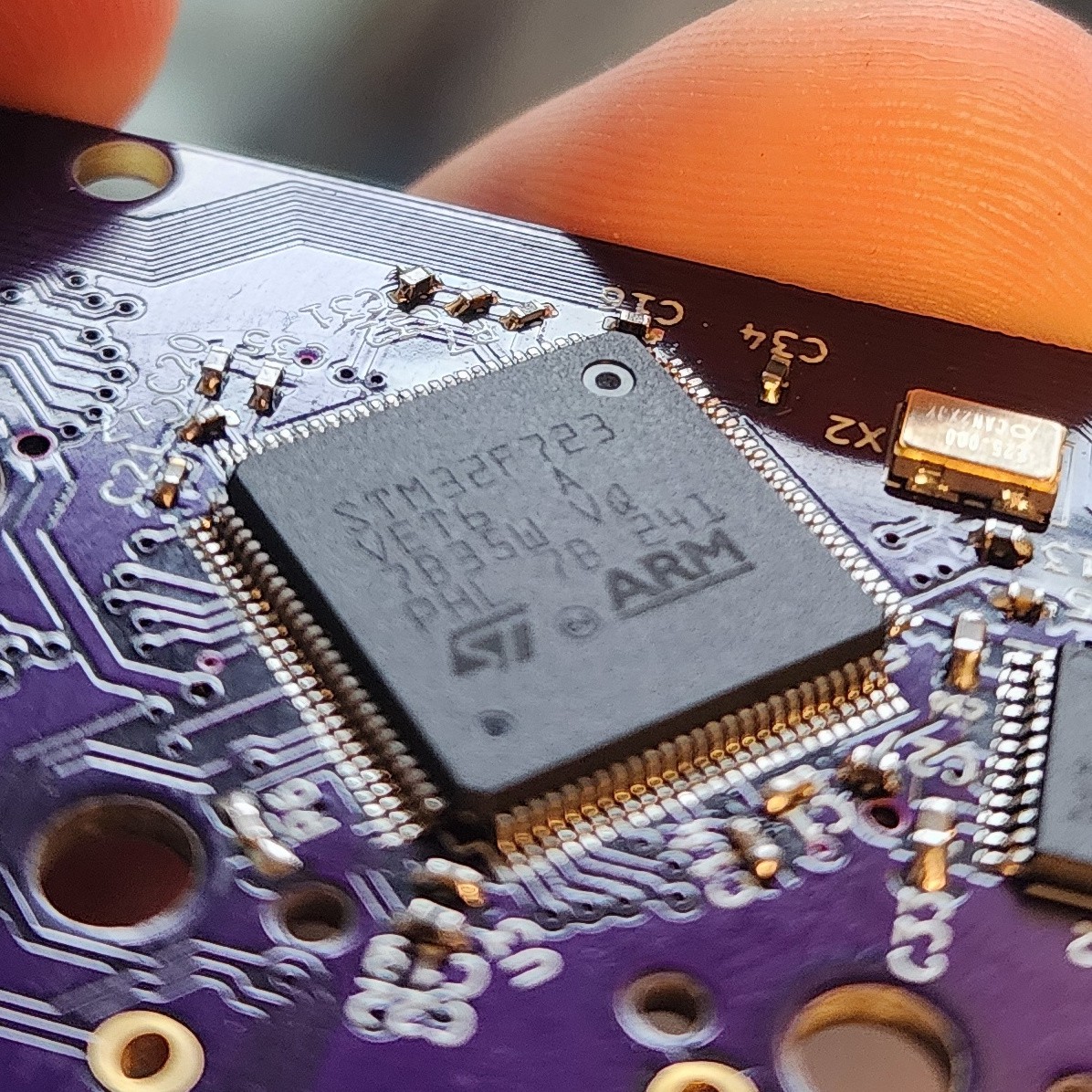
STM32F723 (ARM MCU - USB 2.0 HS)
To facilitate the interface between host and device (keyboard) the STM32F723 was selected. The primary reason for this was the onboard USB2.0 HS PHY which allows for 8000hz (125 uSeconds) interrupt polling from the host computer through the built in HID drivers for Windows, Mac, and Linux.
Having the .125 µSecond interrupt interval is the primary advantage over any current offering on the market right now. All current mainstream keyboard manufacturers Corsair, Logitech, Razer, Wooting, etc. Use USB 2.0 Full Speed (FS) this limits polling to 1000hz or 1ms latency minimum.
USB 2.0 HS also offers another advantage which is that the frame size for an interrupt transfer is 1024 bytes vs the 64 bytes of usb 2.0 FS. This means you now can do NKRO by just extending the number of scancodes in the report descriptor. A.k.a NKRO will send over the state with all of the scancodes included which means no compatibility issues between different operating systems. This method is also boot mode compatible.
NyanOS (NOS) - Firmware 🐱
Nyan Keys based hardware runs on an operating system I created called NyanOS (NOS). This is not based of any RTOS and instead is written in C. This is to avoid any unnecessary overhead that could reduce the performance of Nyan Keys. NOS servers a few responsibilities such as acting as a full featured terminal via USB CDC, as well as prioritizing the HID endpoint over all other tasks. Most tasks are handled as interrupts and callbacks to enabled prioritization via the NVIC.
- USB 2.0 HS HID/CDC composite device
- Serial console via USB
- EEPROM master - FPGA Bitstream Storage
- FPGA bitstream programmer - SPI Master
- Status indication - 5 Leds
- Bitcoin Miner - opt-in
- USB HID Interface @ 8000hz Polling
- SPI Master to FPGA switch serializer and debouncer
The NyanOS out of the box should support any Lattice Ice40HX FPGAs that are also supported by IceStorm. For a complete hardware support list visit. https://clifford.at/icestorm The flow for synthesizing, placing, and routing is outlined below
- yosys <args>
- nextpnr <args>
- icepack <bitstream.asc> <bitstream.bin
- icecompr.py < bitstream.bin > bitstream_compr.bin
The icecompr tool is utilized to compress the bitstream, typically achieving a final ratio of approximately 25-30%. This compression allows an Ice40HX4K bitstream to fit on a 1Mbit I2C EEPROM. Without compression, the bitstream would occupy 131070 bytes, exceeding the capacity of the I2C EEPROM.
In NyanOS, the FPGA is treated as an SPI slave. The system manages all dummy bits both before (8 bits) and after (47 bits) the bitstream programming. NyanOS sends 48 dummy bits to the slave, as 47 is not divisible by 8, and thus it rounds up.
The FPGA bitstream programming in NyanOS occurs at startup and typically takes 2-3 seconds. This duration is primarily due to loading the bitstream from the I2C bus at 200KHz.
NOTE: The time to load the Bitstream is roughly 2-3 seconds and will occur on device power-on. The FPGA can be reprogrammed without a complete device reset, by setting the nos_fpga->configured to false. The main loop will eventually catch this after the interrupts complete and reload the bitstream from the contents of the EEPROM IC that are in Bank 1, using the value stored in the EEPROM bank 0 EEPROM FPGA Bitstream Len address 0x00B0 aligned as 4 Words, where each word is little endian encoded. This will be fixed later but current functions correct and you can use the write-bitstream <size> command and this will all be handled. THE MAXIMUM BITSTREAM SIZE IS 65536 BYTES anything more and you will get a size error returned. User input to keys is not handled until the FPGA bitstream is loaded. Any keys pressed before configuration will not be relayed via the HID peripheral.
Nyan GUI - Software LINK
To configure and control NyanOS in an easy and effective way. I created the Nyan GUI which is a website with a web serial API interface. This lets the user just open up a website in any chromium based browser to configure nyan keys. No need for any driver install.
Below is a screen shot of the Nyan Gui which enables flashing an FPGA bitstream by just opening a file on you host computer! So no need to use any programming tools or special hardware. Just click the cat to connect and then 'Write FGPA Bitstream' and upload your revised FPGA bitstream for better performance or even a different layout! It's up to you. The goal of this is to be highly hackable and modifications are encouraged! Please check this link for the source code to the Nyan GUI LINK
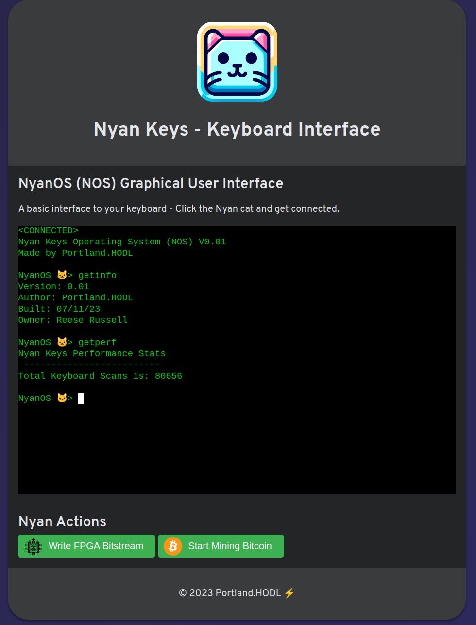
Nyan GUI also has a Javascript based instance of a Xterm terminal that enables the user to start inputting their own commands to hack the cat! A few features I have right now are getting performance stats, setting the owners name, getting build info, writing a bitstream, and help.
Adding commands is fairly easy and can be done in the nyan_os.(c/h) files. So please if you have cool features you want to add to this OS that would improve the keyboard please make a PR in the Nyan OS firmware Github repository.