 fjkraan
This text is from September 2022 when the first board was designed, build and tested.
With clear images of the board and an image of the ROM contents available, it seemed clear that there was enough information available to make a replica. The two main chips, a Motorola MC6803 and a Thompson EF9345 are very well documented with datasheets and more important, application sheets. From this data it would be clear there was only one proper way to connect them.
The 6803 is a simplified 6801 with no internal ROM and just two modes, 2 and 3. The external EPROM indicated it ran in mode 3, extended multiplexed mode. The 74LS373 confirmed this. The EPROM had to be in the upper half of memory space to include the vector space.
The ports P10 to P17 of the 6803 were reserved for the 8 bit dip-switch, Port P20, P21, P22 for mode selection and P23 and P24 for the serial interface.
The EF9345 has its own direct connection for RAM using another 74LS373. So all main pins in the circuit are fixed.
No serious addressing decoding logic is present on board, only inverters. Lots of analog stuff but that is serious way to connect the logic chips. In the end, just one inverter is needed to make A15 a ChipSelect* for the ROM.
The analog stuff is the RS-232c converter and RGB video signal conversion. No need to reverse engineer, enough examples on the internet. A MAX232 solves half of the problem.
A disassmbly of the ROM confirmed its location is in the upper half of memory. All registers of the EF9345 in the lower half (A15 is Chip Select here too, but not inverted).
The situation is complete enough to design a first version of the board. But just soldering it together and see it work is very unlikely. After a long period of thinking (and working on other projects), the solution was to create a custom 6803 exerciser. Having done this before for a Z80 and 6809, it would allow checking the circuit board without processor. The exerciser doesn't do instructions, but just handles pins. In isolation, but also in combination. So Read and Write operations could be executed and monitored.
The Exerciser is build upon a Arduino ATMega2560. The program is trival (having most of the routines already in written and tested).
*1) But what the dip-switches do has to found out. A working configuration is known from the images. Really interpret and annotate the disassembly is (not yet) required.
The board was created in September 2022 and I figured it was too complex to assume it would work by just putting all components on the board and apply power. After all it was my own, untested speculative design.
The best I could do was try to test parts of the schematic in isolation and only then add an other part to test.
- The first part was the RS-232c interface. As it was just a MAX232 and some capacitors. The Exerciser was used to toggle1 the P24 pin (TX)of the 6803 socket, connect pin 1 to pin 2 of the SERIAL header and check the result on the P23 pin of the 6803. This worked2.
- Next step was to check the EPROM. This includes the address latch U2 and inverters U1. Here I discovered the EPROM databus was connected in reverse. This resulted in the purple patch lines at the boards solder side. This illustrates the limited confidence in my own designs.
- The third step was testing the dip switches. These worked, but I found a loose contact in the Exerciser to 6803 socket cable. The DIP-socket numbering is in reverse, but that is like the original, so Ok for now.
*1) Q9 to get a 512ms square wave, B#P24 to exercise pin P24,
*2) Used the "TTL voltage level probe" for this.
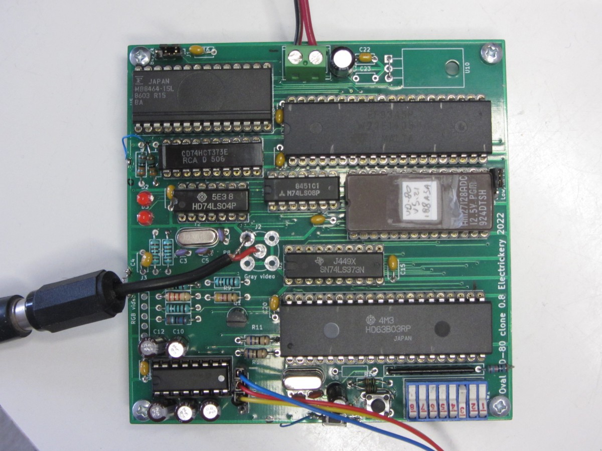
This is the first board, 0.8, which worked after extensive fixes.
Discussions
Become a Hackaday.io Member
Create an account to leave a comment. Already have an account? Log In.