 sky-guided
Whipped up a prototype PCB in KiCAD, ordered a batch of parts from Digikey, all set to go, yeehaw.
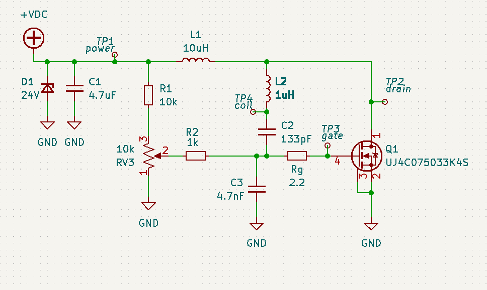
(not pictured in the above schematic: power LED and some other board affordances.)
Of course I knew that this probably wouldn't work first-time, but I still held out hope.
There's some ugly design compromises -- in particular, the 1k through-hole resistor is doing double-duty as a jumper wire. I increasingly prefer to prototype with surface mount parts whenever possible, but this board was an odd mix of SMD and THT. The bank of 5x capacitors (marked C2 on this board) was intended so I could easily adjust the total value of C(p) and to spread heating between multiple components.
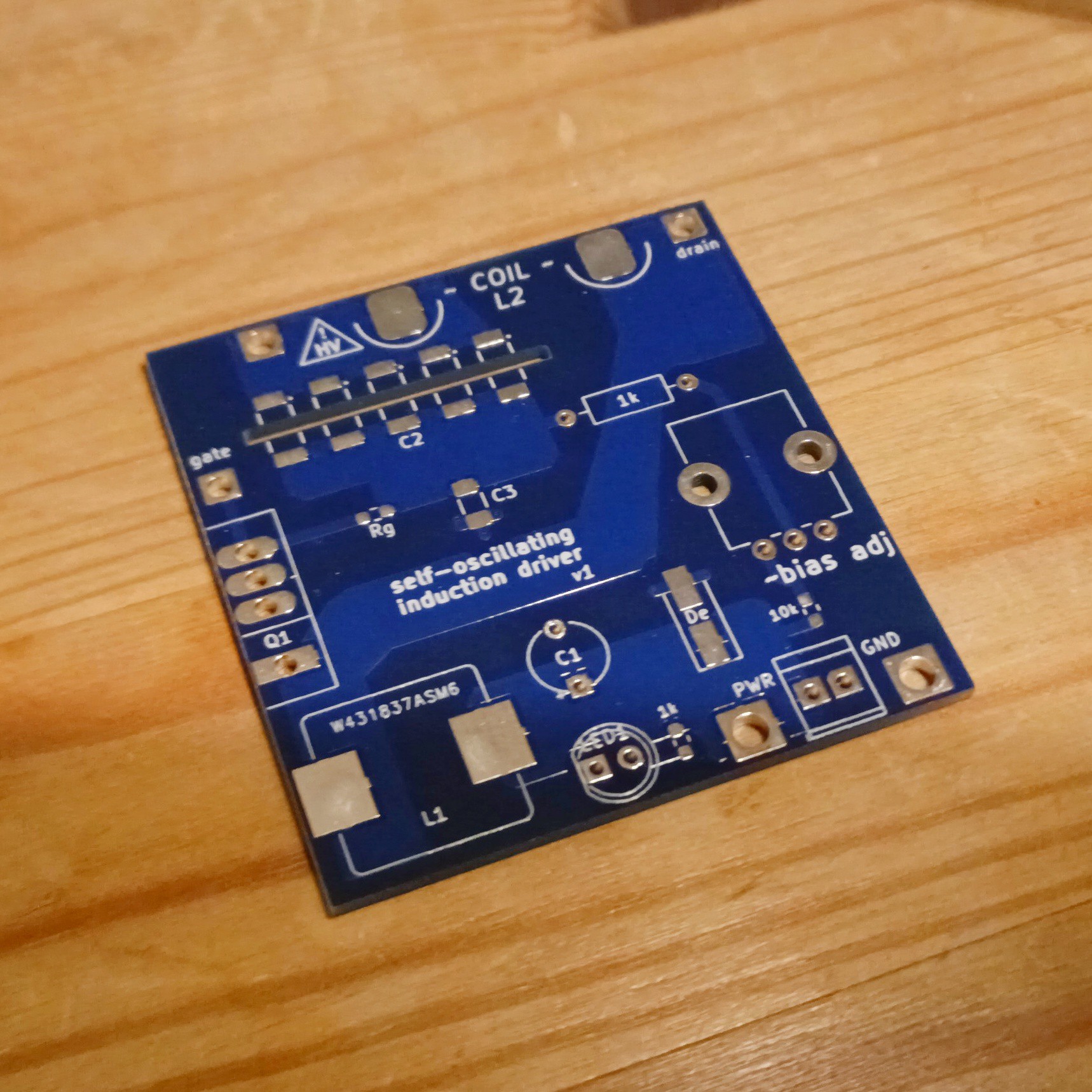
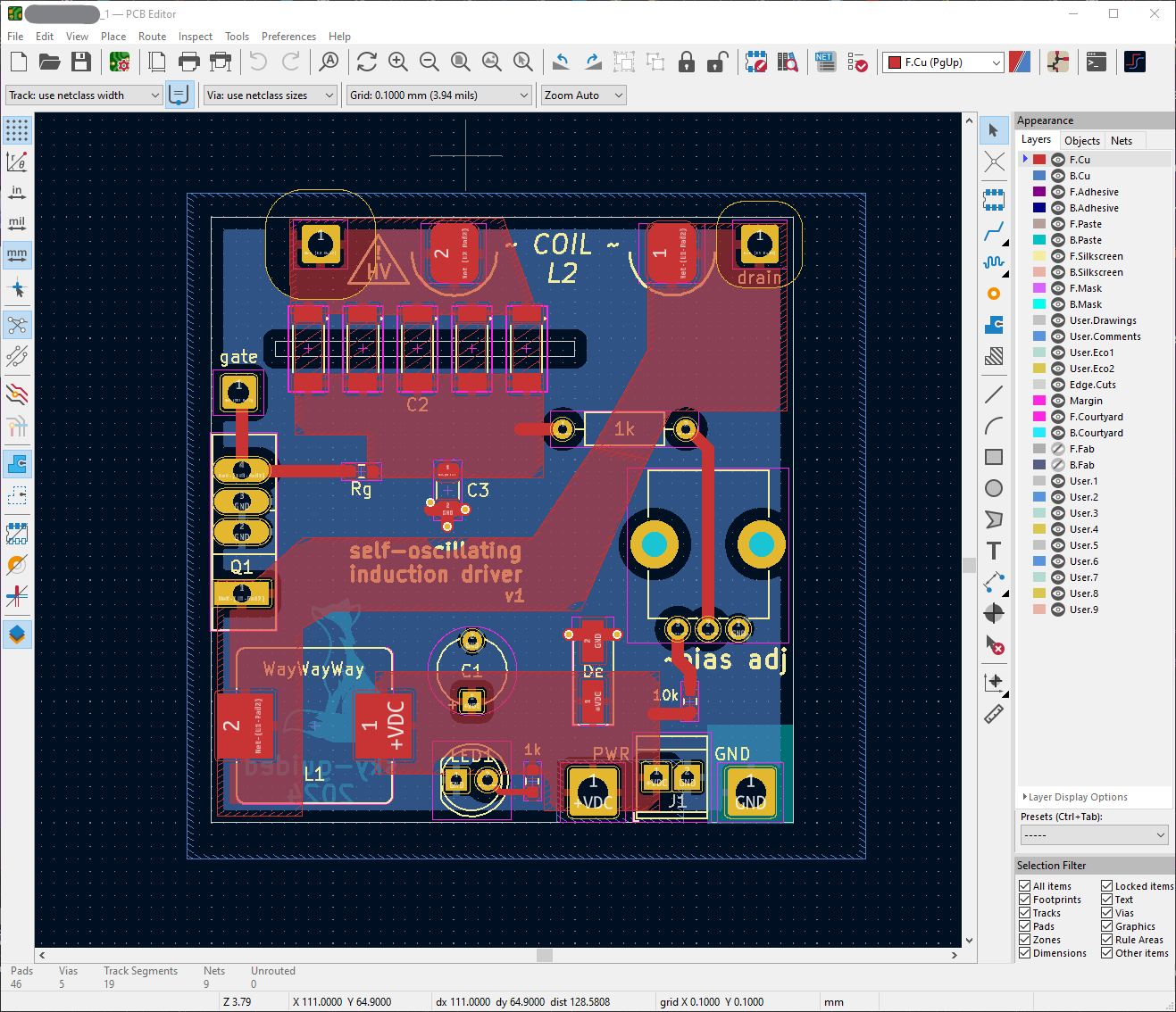
Decent boards, blurry photo.
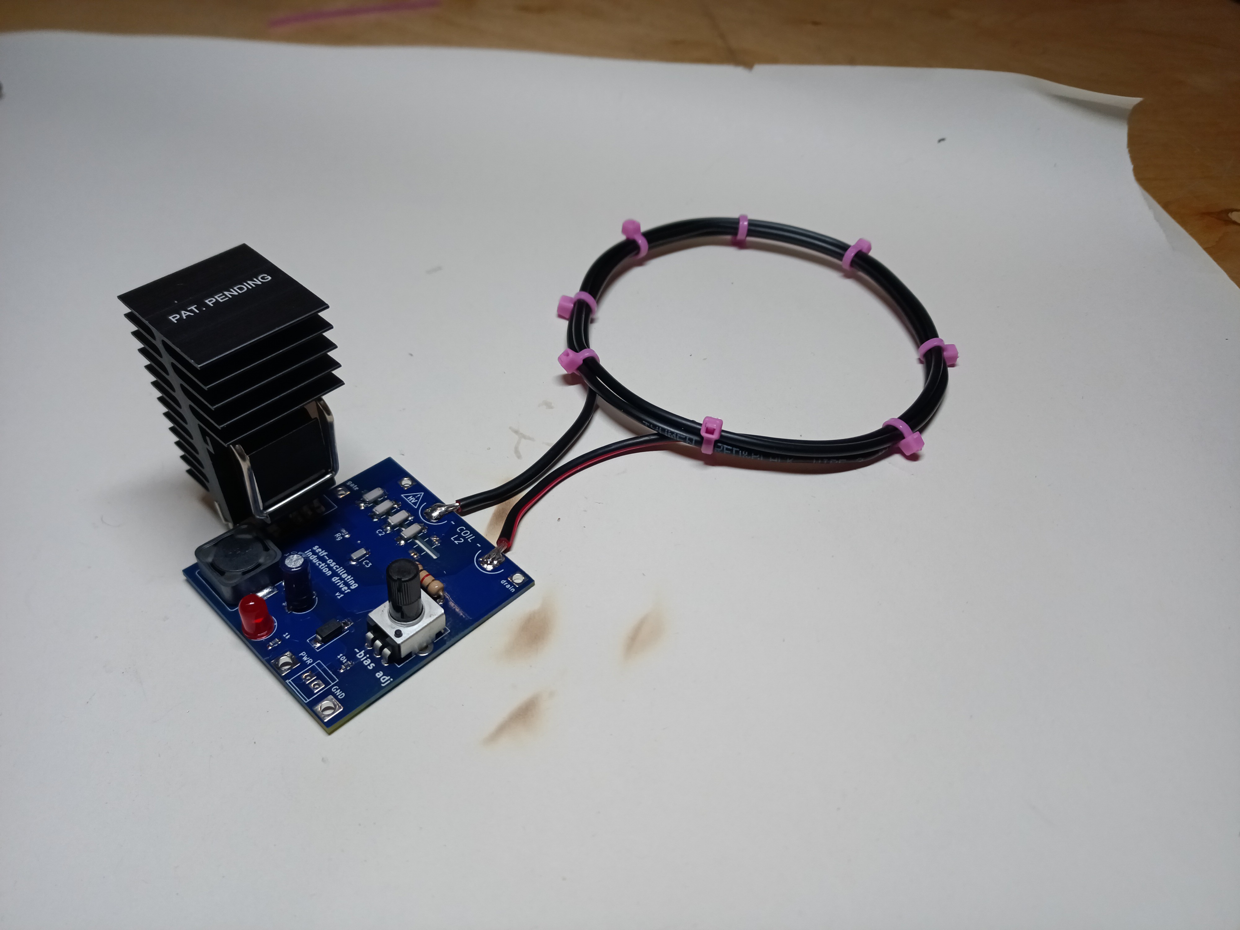
Assembled easily enough. This first coil was three turns of 18ga wire.
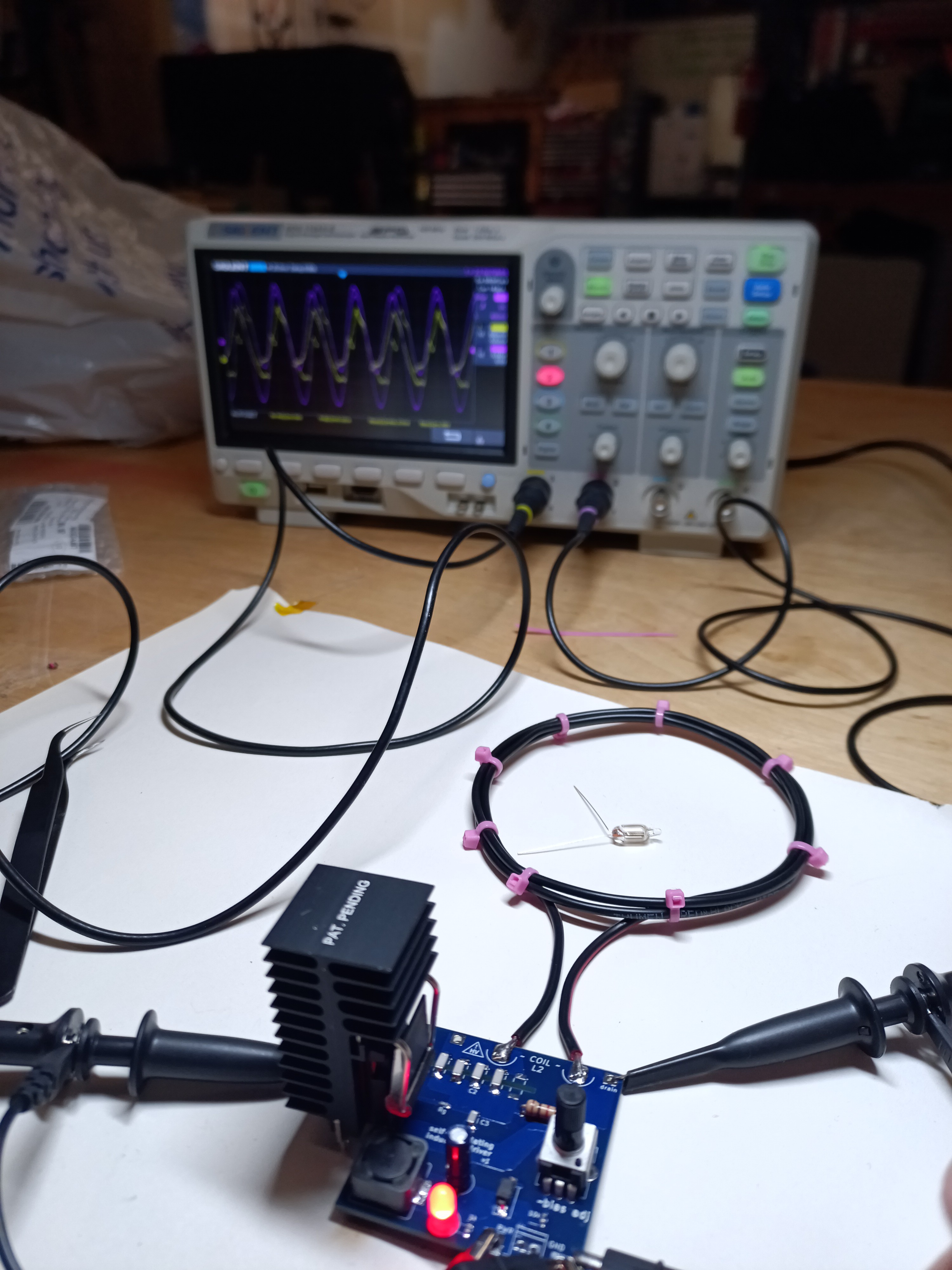
Things got going with some kind of oscillation, but definitely not what I was looking for.
At this point I blew my first mosfet. The mosfets I'm using are the UJ4C0750-series new-hotness SiC FET's from Qorvo, and they're not particularly inexpensive. The THT mosfets used in this first prototype were also fairly annoying to replace, since the holes barely had enough clearance diameter and solder was hard to sufficiently clear out.
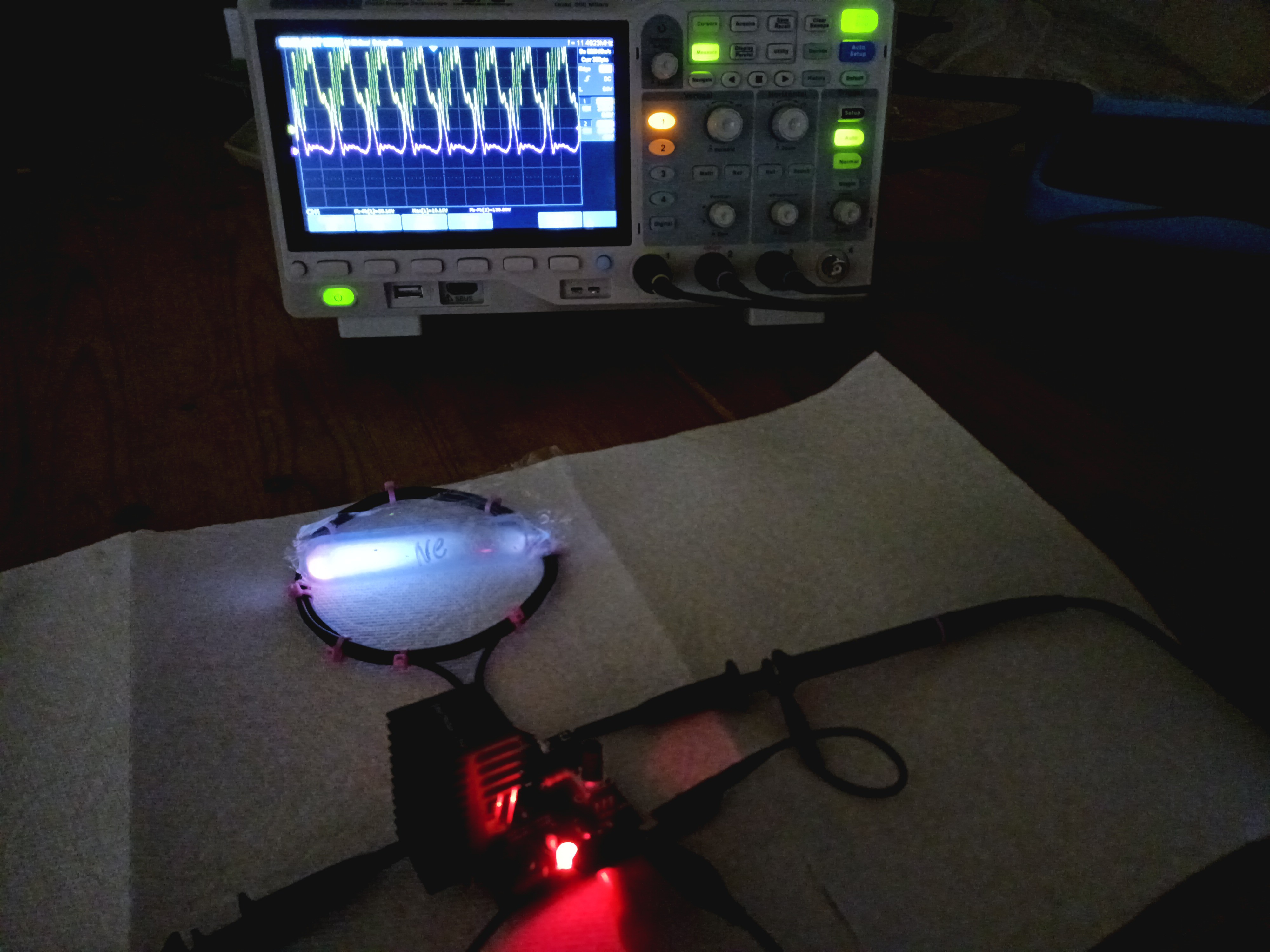
Changing C(g) from 22nF to 10nF (almost) got me the intended waveform! Since my 1L xenon globe from Wayne Strattman hadn't arrived yet, I was illuminating a small ampoule of neon.
There's clearly some kind of ripple on the gate (yellow trace). I measured that to be somewhere around 100MHz, but unfortunately I don't have good oscilloscope printouts for these first trials.
Blew up another mosfet when bending the coil while the circuit was running, and somehow blew up a third trying to probe the HV coil voltage (and possibly smoked an o-scope probe in the process -- really should have noted its voltage limit first). I'm guessing I got some kind of inductive kick at loss of oscillation?
A big deficiency in this first prototype is there's no voltage protection on the gate.
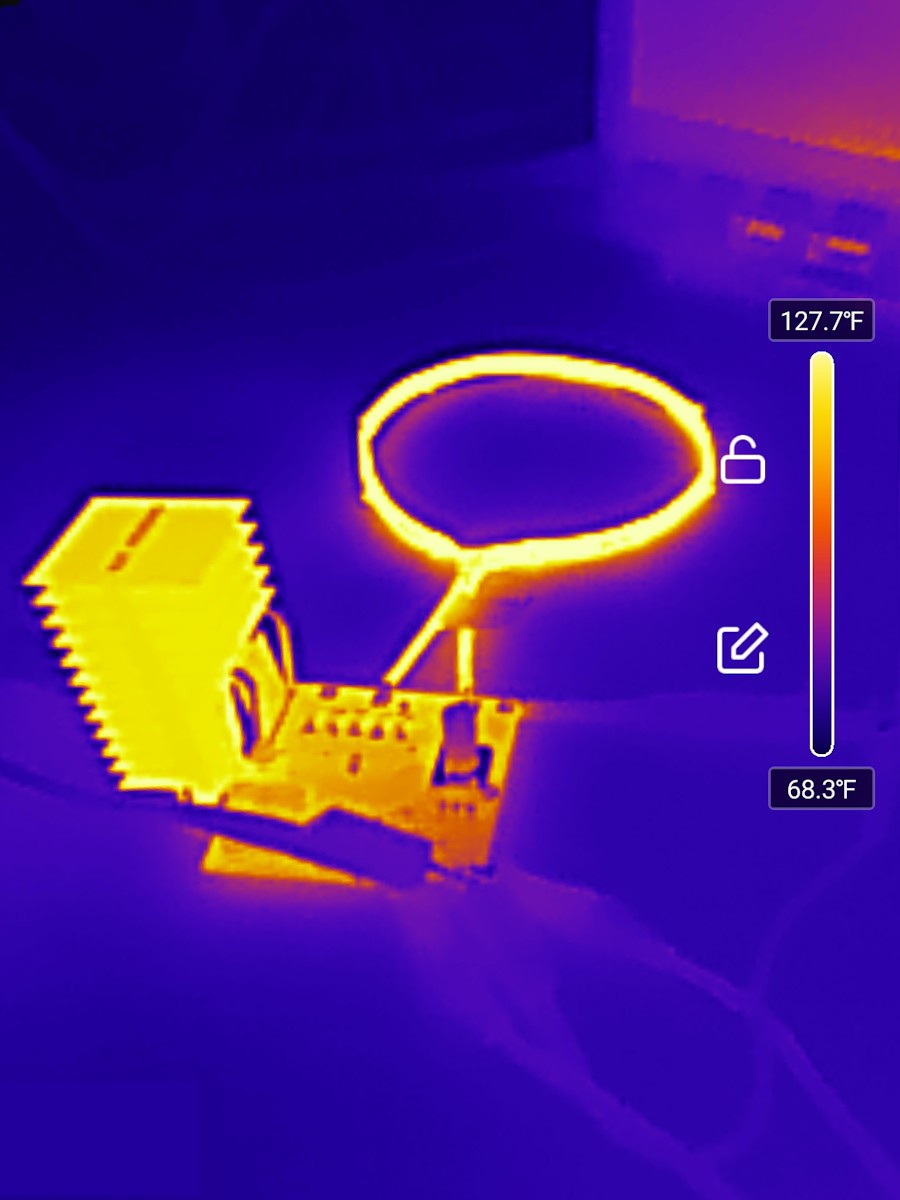
Component and mosfet temperatures stayed pretty reasonable, but the coil got very hot very quickly. In retrospect the cause was obvious -- skin effect depth at these frequencies is only about 20 microns, and the top 20 microns of a 18ga insulated wire just isn't enough conductor.
I made two more inductors, this time actually characterizing their inductance. The first was a tight 1.3uH coil designed to wrap around one of the ampoules in the hope that I could see at least some inductively coupled plasma before my xenon globe arrived. LTspice said that inductance value should work fine, but instead my mosfet instantly failed short.
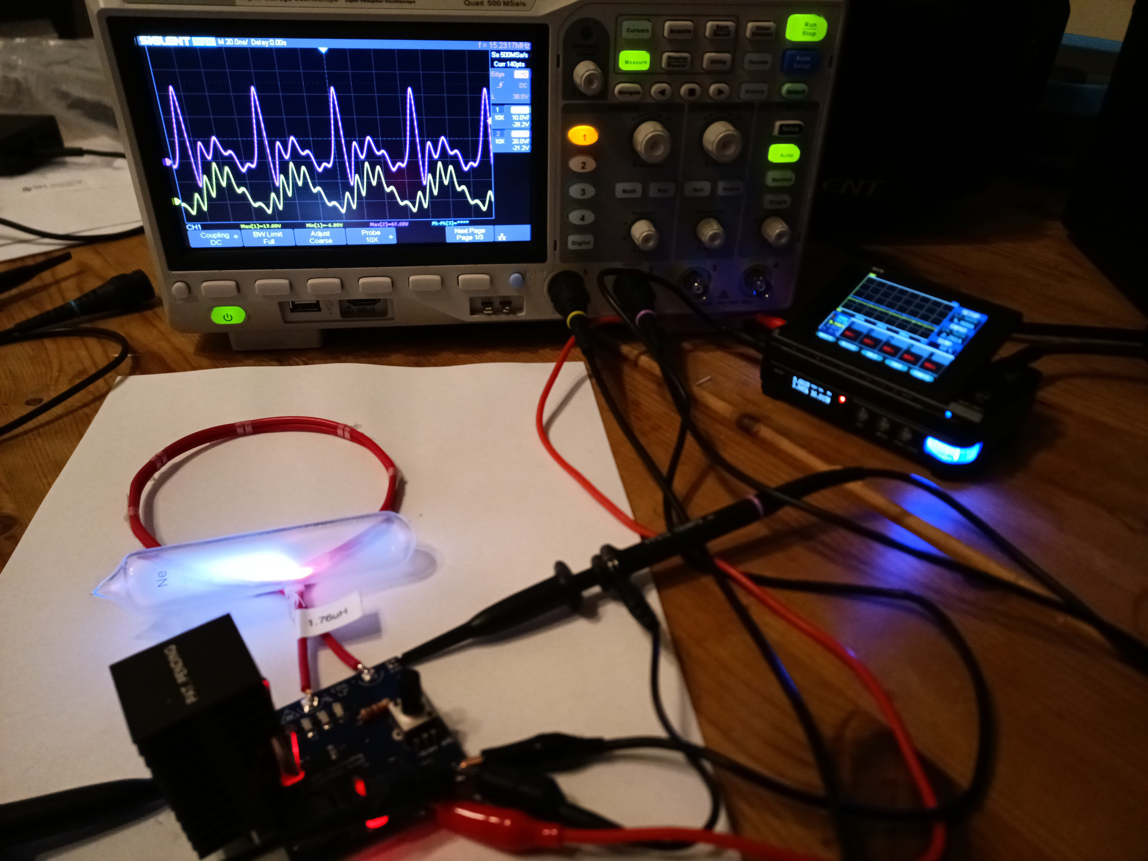
A two-loop coil of ~1.8uH worked, but the switching is clearly messy (pictured here at 12V supply). The big motivator for investigating a two-loop coil was my intent of using a two-layer PCB as the inductor in my final design.
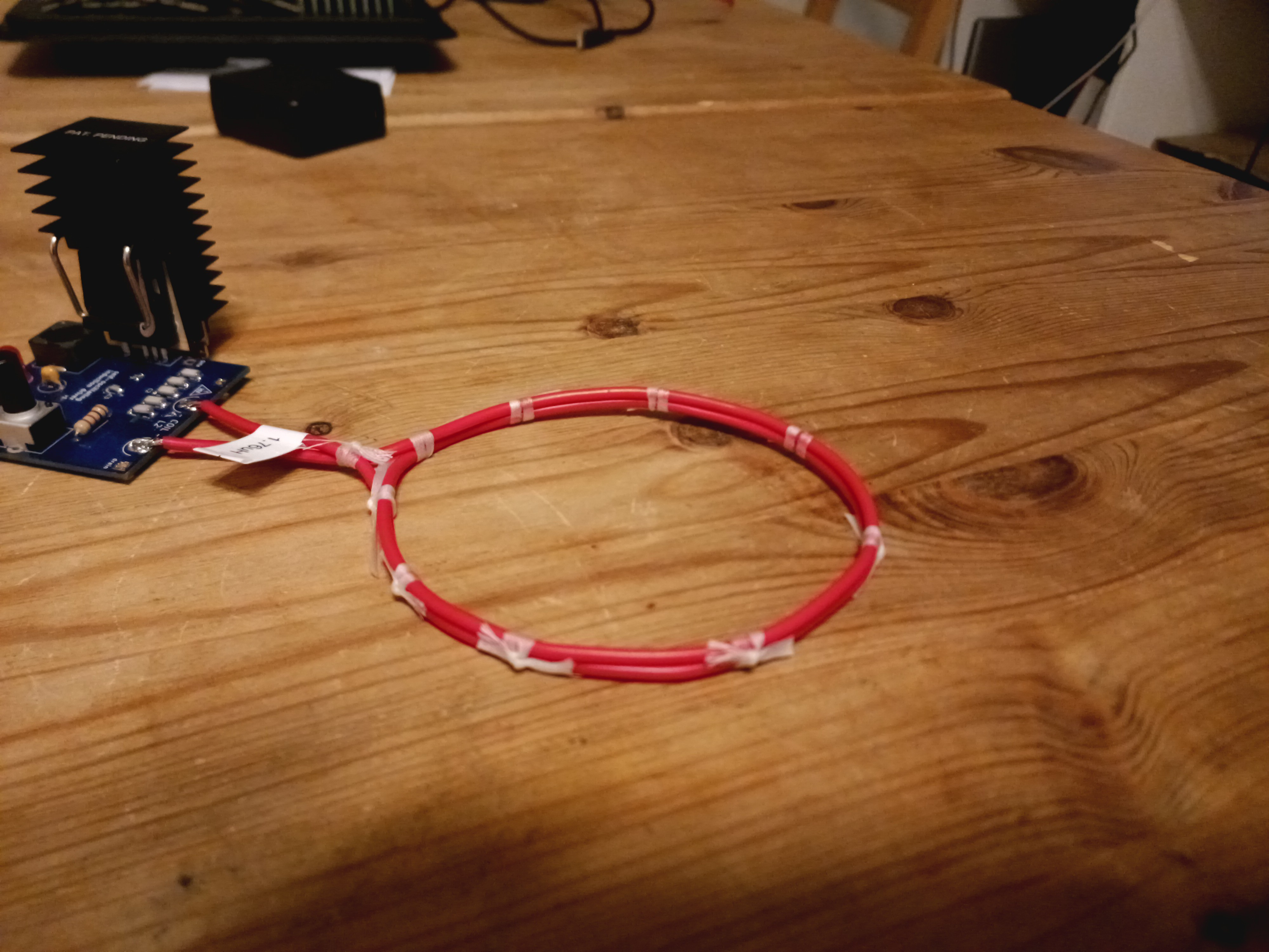
Using lacing tape does make the coil a lot nicer than zipties, at least. Lacing tape is great and I wish more folks knew about it.
And... I blew my last mosfets screwing around with different drive voltages and component values. RIP.
Version 0.2 is coming soon.
Discussions
Become a Hackaday.io Member
Create an account to leave a comment. Already have an account? Log In.