 MS-Dzo
 Hello everyone !
Little update on the DAC, let's see what we have in store for today.
1 - Prototype Topology
First things first, Since i'm doing an output stage, i'm going to have to deal with differentials filters, differentials amps, power supply filtering etc. The board will include those elements, but they'll be somewhat isolated (i need to test them after all ! ). The entire thing will be powered by a stabilized power supply, so expect banana plugs and BNC test points.
Since my outputs can be differents (bridge tied vs single ended), It means that I will have to use AD and BD modulation.
For testing, i also want a mono single ended output.
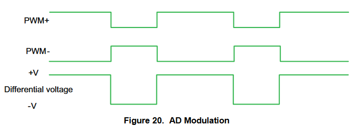
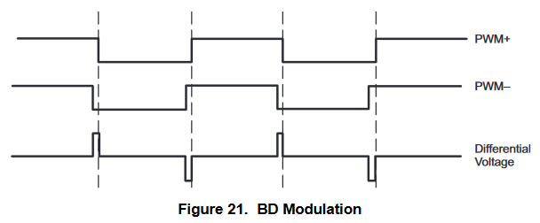
(ripped straight from the datasheet)
most headphones lines are single ended and not differential (Left and Right share a ground) so that's what i'm going to design at first.
2 - Filter Design - Single Ended output
Let's start designing ! the datasheet says that the output PWM frequency for a 96kHz 24 bit audio signal will be over sampled x4 which is 384kHz. That's a lot less than i expected (I would have thought it'd reach the MHz range). So, i think a higher order low pass will be needed because i doubt -20dB will cut it to remove all those high frequencies harmonics.
I know the actual speakers can't reproduce those sounds, i'm mainly focusing on the EMI produced by all that switching over the cables.
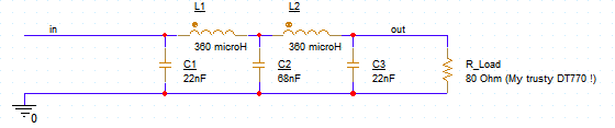
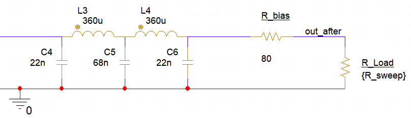
Might aswell go overkill, so here's my attempt at a 5th order Butterworth filter with a ~60KHz cut off frequency. I chose this frequency such that any ripple that happens after normalizing the components values would be ideally after 20KHz.
I ended up with a sliiiight ripple but it's inevitable, and check this out, -72dB at 300KHz. Take that high frequencies !
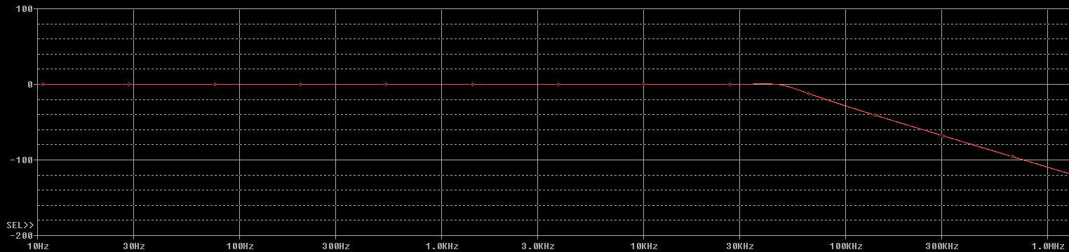 As for the ripple, it should be perfectly inaudible at 20KHz since it's only -0.007dB !
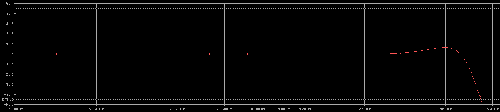 Turns out having a whole semester about butterworth and chebyshev did prove useful after all, uh.
By the way, the impedance of this filter is 80 Ohms because the headphones are use are 80 Ohms too, but after all, it doesn't really matter ! (haha...)
Should i add a ferrite for EMI too ? i don't know ! Here's the circuit.
please comment if you know more than me (you probably do !) because this filter design seems good enough for me...
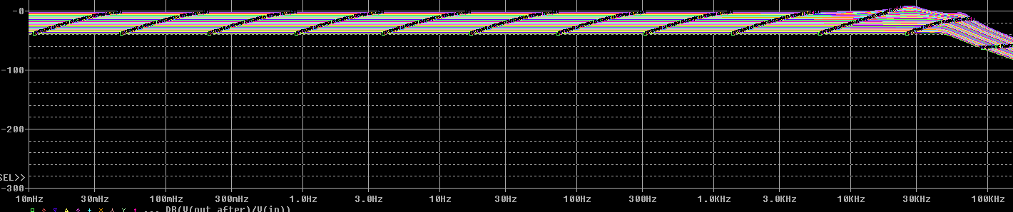
Wait... you hear that ? Holy jesus...
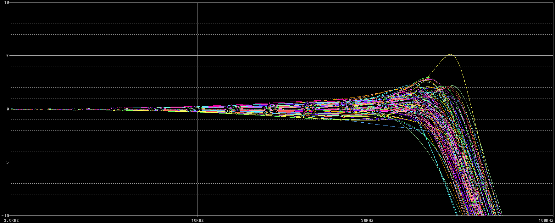
What is that ? What the fuck is that ? That my friend is what happens when you do a hundred runs of monte carlo analysis with a 10% margin on error on all 5 components of the filter.
So, three ways to deal with it :
- stop with the high order stupidity (i don't wanna :c) and pay more for 1% components (the results are good enough tbh)
- find another filter design that is less sensible to single component value deviation (i don't know any)
- place the capacitors next to each other to mitigate thermal effects as much as possible, while also trying to pick the best matching ones myself.
I'll go with solution one and three thank you
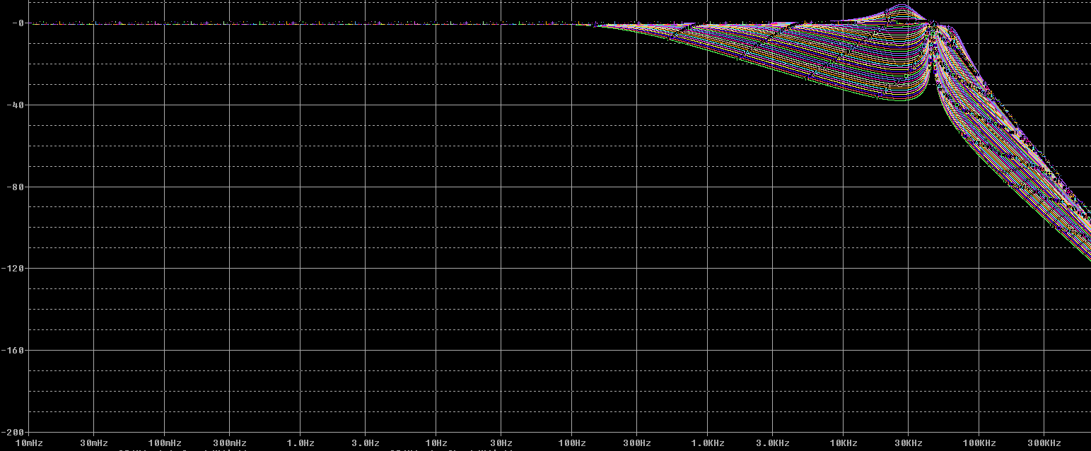
Did you know that headphones impedance can reach as much as 600Ω ? Here's the response with perfect components but with variable output impedances (from 1Ω to 200Ω) :
 and, just to test something, here's a second order LC low pass filter response for an impedance varying between 1Ω and 1kΩ
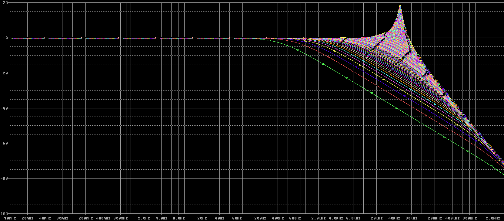
Uh oh....
3 - Load dependency - Buffer Stage ?
So, changing the load changes the frequency response : if you plug your fancy 200Ω headphones to my nice 80Ω filter, you get -40dB (x0.01) of the sound level at 20kHz. This won't do !
The easiest way to deal with it is obviously to put a resistor in series or parallel depending on the load value , and make it variable : if your load is 2Ω then your resistor should be 72Ω in series so that the entire impedance is 80Ω. you'll get a lot of attenuation but the frequency response will be ok.
As you can see, the traces are almost the same even if the load changes, they're just offset.
This would be a good solution if i wasn't going to make an output stage for big subwoofers and whatnot down the line : if I want to output 100W then i need a resistor array rated for 100W. Still, i guess this is beyond the point for now because I'd also need a filter capable of handling 100W.
One would think a voltage follower should be usable, yet the biggest issue is that the entire point of a voltage buffer is to have a high input impedance and low output impedance, effectively nullifying the work of the comparator amplifier, and circling back to an inefficient class A amp !
After talking with some analog wizards the answer i was given was essentially "If you want a filter, you need one for all range of loads you want"
So, here are the different solutions we've agreed on:
- ditch the pure class D design and go with a Class A output stage
- ditch the high order filter, try to use a ferrite bead.
- create a filter bank, where each individual filter work for a small load range.
- scrap the whole idea entirely and go full analog
It's true that the higher order filtering isn't actually done on all the literature i've found. even datasheets only mention simple low pass LCs, which heavily imply that it's not needed at all :
 for the engineers behind the MD7120 , a simple LC is sufficient for a bridge tied load with PWM inputs.
I'll design a a high and low order filter and check the effect of not filtering the HF with the EMI probes available at my uni, so until then it's a moot point ¯\_(ツ)_/¯ i'll just allow for switchable filters on the prototype PCB with jumpers. I'll also add a ferrite bead in serie that might (or might not) work. since i don't know what the effects will be and if it can withstand the power, i'll also make it selectable with jumpers. i've decided on a KEMET B-01
Here's the circuit !
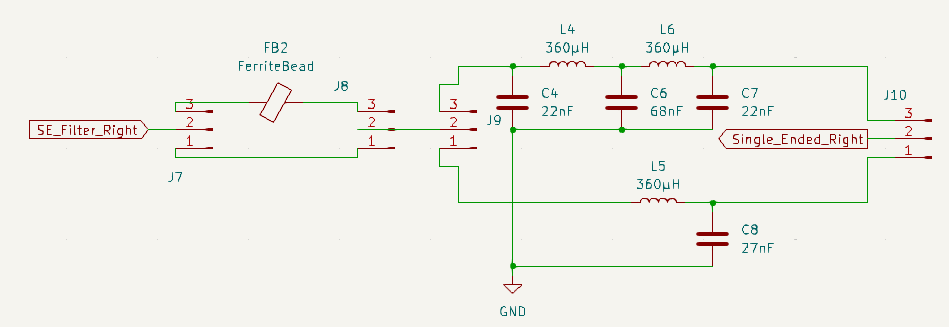
The right channel single ended filter is the same, and both connect to a 3.5mm jack.
I'll implement a selectable filter array, so honesty i think going the 2nd Order LC is the way to go
4 - Filter Design - Single Ended filter bank selection
We need to be able to connect and disconnect our filters (remotely). There are 3 topologies that i have found, but one of the will be a real bore :
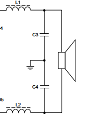
1 . Series inductor, disconnecting the caps
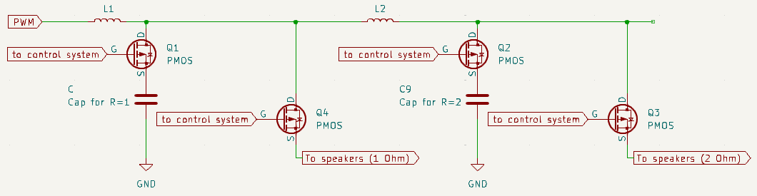
basically, by turning on/off the transistors, we let the signal go through a specific amount of inductors, the sum of which give the cut off frequency wanted. a single cap is also selected, and a path to the speaker is made.
It's perfect in theory, but there's a few problems imo :
- the "control system" needs to give a high enough voltage since it's on the high side.
- the inductors aren't perfect, but their value needs to be really precise. they vary with temperature etc. so matching all of them will be a pain.
- the system isn't modular at all. if you have a filter for 1,2,4,...,100 Ohms and you want to add a filter for 3 Ohms then you need to redesign, remove and rewind all the inductors from L4 to L100.
For a perfectly static system i think it'd work, but i'm looking for something modular, since i frankly don't know what i'm doing and will probably need to tinker and bodge over and over. I'm not looking to redo more of my work since that's pretty much garanteed already.
2 . Latching relays : straight forward solution
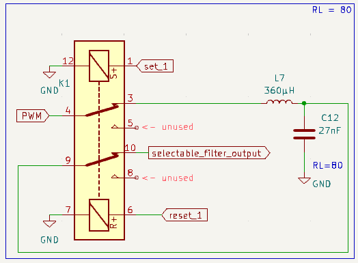 Relays are kinda pricey, but overall this is a much more modular solution. a bank of those modules can be selected with the sets and resets (i've omitted the flyback diodes in the diagram).
One issue though, each filter needs its dedicated relay, but this can be cut down with using the "off" ports (marked unused on the diagram)
3 . Latching relays : Multiplexing
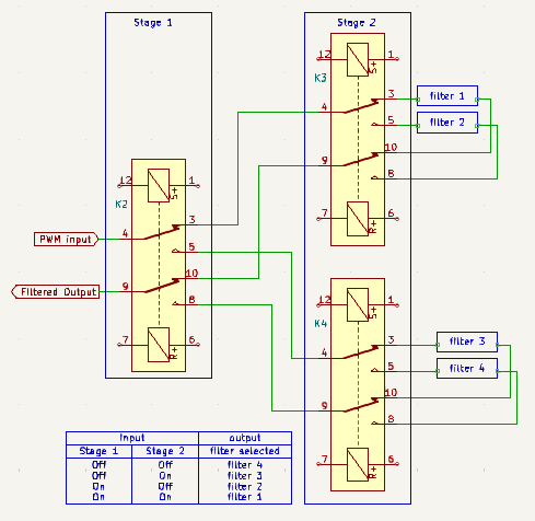
This method is a tad more efficient if you want an amount of filter that is a power of 2: you always need one less relays than you have filters.
Both solution have their own ups and downs : this one is less efficient if you have an odd number of filters, it offer less modularity...
As we're still prototyping, i'm going with solution 2 !
4 . Same thing as before but with MOS as switches
I'm not against that idea, but all the biasing will be a pain. Our single ended speaker is connected to ground, so we need to separate it from the filter bank by placing the transistor on the high side, which needs a high enough voltage.
Here are the final schematics for the test circuit :
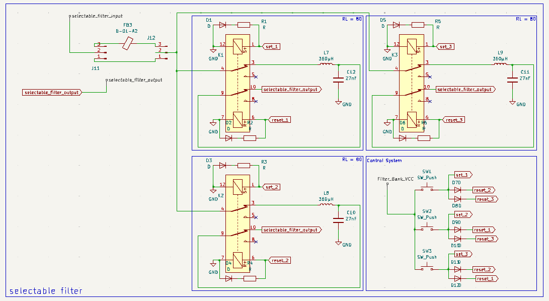
Filter bank selection module (value aren't different)
That's it for today ! next time we'll design the BTL differential filters !
As always, if there's a huge flaw i haven't seen or you have ideas / remarks, feel free. Cya !
Discussions
Become a Hackaday.io Member
Create an account to leave a comment. Already have an account? Log In.