Close
0%
0%

Λ M U L E T motion controller

High-performance open-source BLDC controller compatible with moteus firmware.

Similar projects worth following
The Amulet motion controller is a high-power brushless motor controller compatible with the moteus firmware. It was specifically designed to be integrated in custom quasi-direct drive (QDD) actuators for a legged robot.

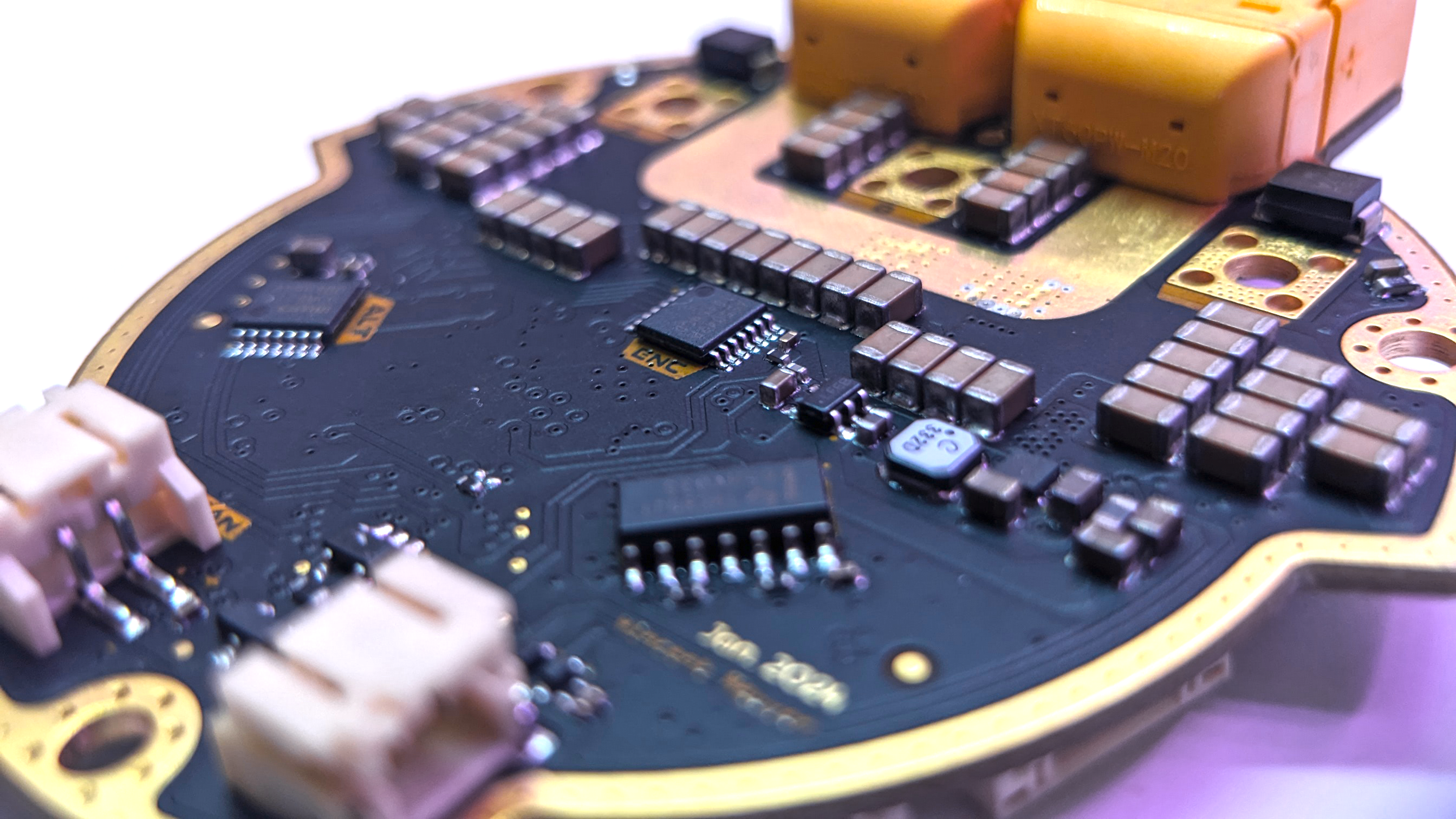
Amulet was developed specifically to be integrated in our custom quasi-direct drive actutators for a quadruped robot. We've decided to develop our own motor controllers to have the highest amount of flexibility when it comes to some of the most crucial hardware. 

The amulet controller is a modified version of the moteus controllers, providing higher peak power, thermals and cooling capabilities and more. It runs a modified fork of the moteus firmware.

NameΛMULET V1.0
Voltage Input12-44V
Peak Phase Current100A (to be further tested)
Peak Electrical Power1500W (to be further tested)
Communication5Mbps CAN-FD
CoolingLow-side switched 12 fan
Positioning2x Onboard 14-bit Encoders
PWM Switching Rate15-60kHz
Control Rate15-30kHz
MCUSTM32G474
Dimensions69.7 x 76.7mm
MassTBD

  • RC snubbers

    Nguyen Vincent03/31/2024 at 16:32 0 comments


    To reduce ringing, I've added optional RC snubbers in the design. They are placed as close as possible to the FETs, but due to limited space, I was limited to using 0402 for Csnub and 0603 for Rsnub. This limits the maximum dissipated power in the snubber.

    Before adding snubbers:

    After adding snubbers:

    I have decided to use 5 ohm 0.4W for the resistor, and 3300pF for the snubber capacitor. This proved to be a good balance between power dissipation and oscillation dampening. A good ressource for snubber tuning can be found here. The chosen passives result in an overshoot of around 4% compared to 8-10% before adding the snubber.

    Currently, I estimated the dissipated power in the resistor using 


    Where α is a derating factor between 0 and 1, usually around 0.43 (see Correct Snubber Power Loss Estimate Saves the Day). With a frequency of 30kHz at 44V with α = 1, this results in a power dissipation of 0.19W.


    When measuring high-frequency signals such as this one, it is important to use a probe with the lowest amount of inductance (i.e. with a short ground clip). As I didn't have such a probe on hand, I had to improvise something:

    This significantly improved the maximum bandwidth that could be measured. However, it would be a good idea to redo the measurements with a faster oscilloscope.

    With standard ground clip:

    With handmade ground clip:

  • Power sequencing - validation

    Nguyen Vincent03/24/2024 at 16:34 0 comments

    A power sequencing scheme was designed to ensure deterministic behavior on power-up. The regulators are sequenced as follows:

    It is important to validate the power sequencing experimentally, to estimate the time needed for the board to be in a working state. The scoped signals are as follows:

    It can be seen that the power sequencing does not exactly follow the initial estimation. The most notable discrepancy is in the +A3V3 power rail (low-noise 3V3 rail), which has some sort of soft-start feature. This is an important feature to note, as the moteus firmware uses this rail as a reference for ADC measurements at boot-up, to determine board family and version.

    The modified power sequencing graph is as follows:

  • In the flesh - finally some prototypes!

    Nguyen Vincent03/24/2024 at 16:26 0 comments

    Thanks to PCBWay, which kindly sponsored 200$ for this project, I recently received a fully-assembled board (minus the through-holes which I decided to assemble myself). You can see a few pictures here:

    Working with PCBWay was quite pleasant. They send you pictures and confirm component placement and polarity with you before shipping.

    The quality is great, and assembly process was quite smooth. There were a few issues for component sourcing, but they were quickly resolved after communicating with one of their engineers. The board worked on the first try with no issues.

  • More details on the layout

    Nguyen Vincent03/24/2024 at 16:17 0 comments

    Stackup

    The board is comprised of 6 layers, using the following stackup:

    LayerThicknessFunction
    L12ozSIG/PWR
    L21ozGND
    L31ozSIG/PWR
    L41ozSIG/PWR
    L51ozGND
    L62ozSIG/PWR

    Where L2 and L5 are solid ground layers. It is important for good signal integrity and EMC to have solid ground planes next to each power and signal layers. The stackup was chosen to respect such a constraint and maximize the number of power layers (which are parallelized for higher current carrying capacity).

    Layout

    Layer 1

    r/PrintedCircuitBoard - L1 (SIG/PWR)

    The first layer is mostly comprised of signals, and is the only impedance-controlled layer. Impedance control is not strictly necessary in the scope of this project, but we decided to use 100-ohm controlled impedance for the RS422 and CAN interfaces. 100-ohm was chosen instead of 120-ohm for CAN because of manufacturing capabilities (120-ohm would require track width/spacing that would increase the price).

    Initially, I tried to place the CAN transceiver and termination resistors as close as possible to the connector to reduce the length of the stub. In the end, I decided to place them just below where I believe are the large ground return paths, to avoid ground shifts on digital lines. Before the transceiver, the CAN lines are in the form of a differential signal, which means that they should be quite resistant to common-mode noise.

    The gate drive signals were routed to minimize inductance; short and wide tracks, with the associated return path close to it. In the case of the high-side drive signal, the return path is referenced to the drain of the high-side FET. Ideally, the gate drive signals should be routed in internal layers to reduce potential noise radiating outside of the board. However, to keep them from splitting the +VBAT polygon (in pink), I decided to route them on the outer layers.

    A high clearance is kept throughout the board according to IEC60664-1 where possible. 

    Optional RC snubbers are placed close to the FETs to reduce ringing during switching. A further log will discuss its impact on the phases' PWM signal waveform.

    An interesting thing to note is the top part, which can be broken off if a more compact footprint is desired. It is then possible to solder wires for power and CAN.

    Layer 3

    r/PrintedCircuitBoard - L3 (SIG/PWR)
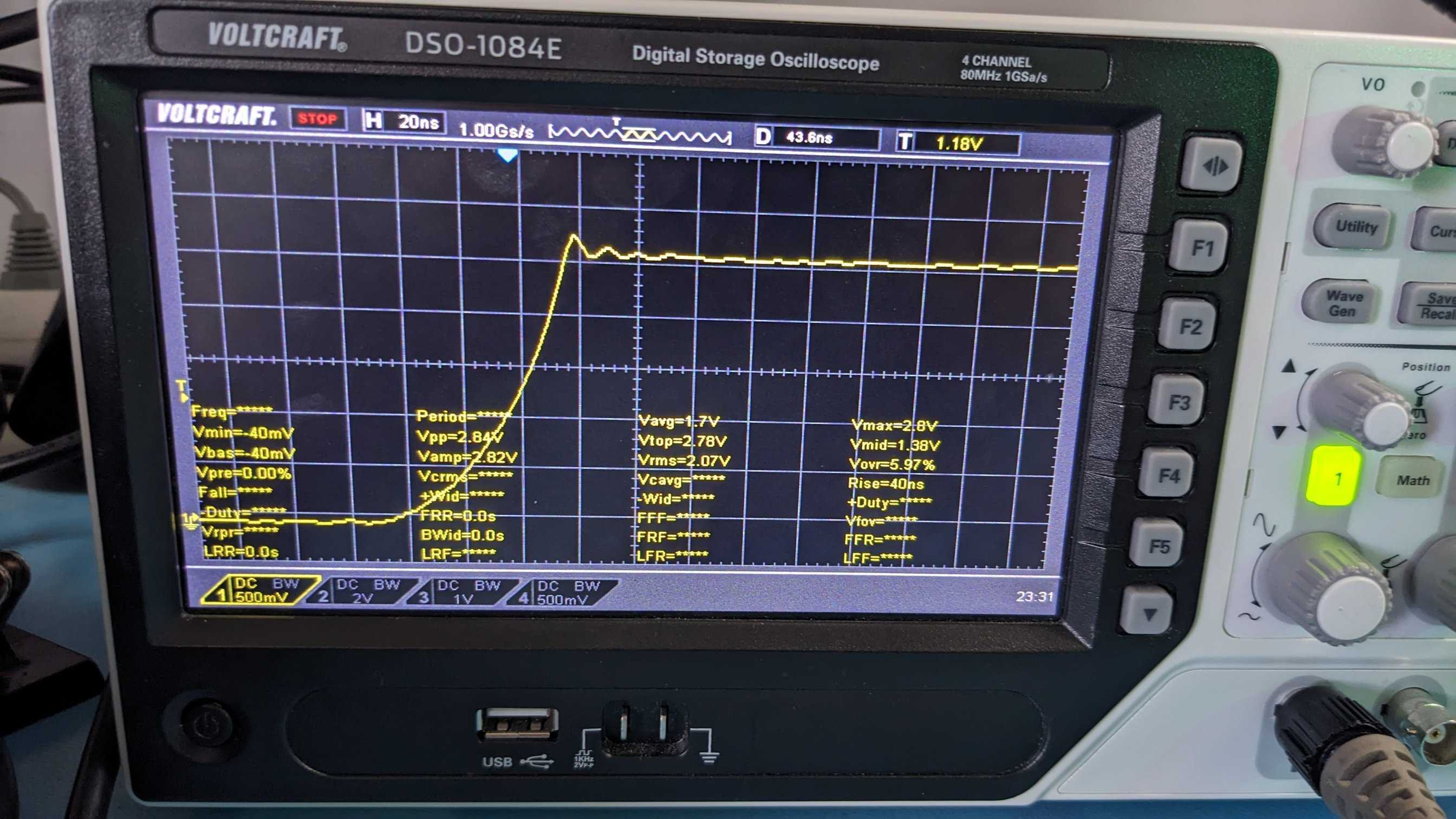
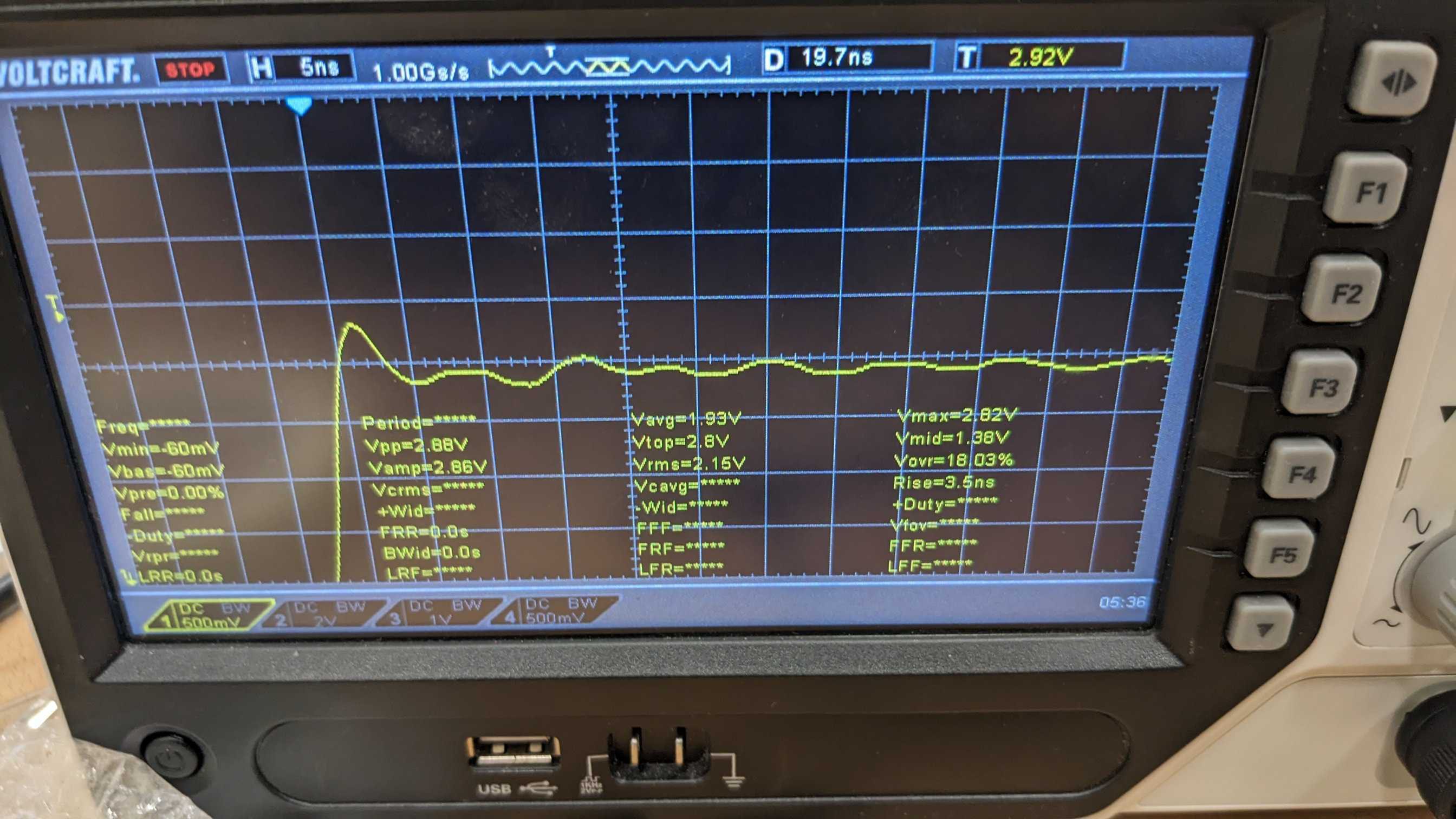
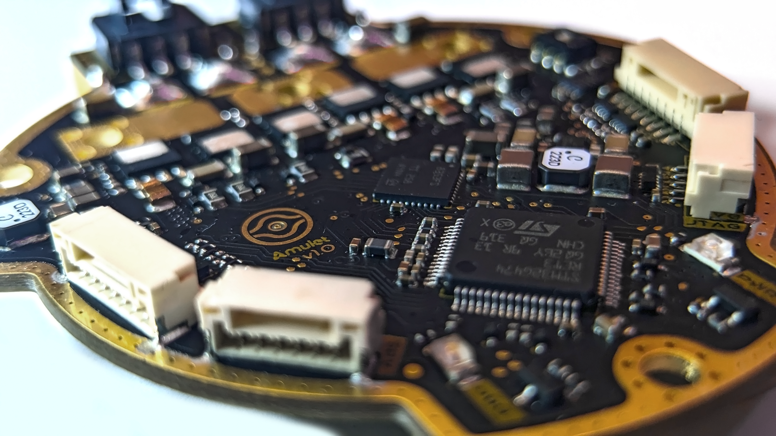
The first inner layer is dedicated to analog signals and a few power planes. special care was taken to route the kelvin sense connection as far as possible from noisy signals. They are surrounded on both adjacent layers by a solid ground plane, and no return currents from any layer are present in the ground planes above and below the kelvin traces.

    Layer 4

    r/PrintedCircuitBoard - L4 (SIG/PWR)Special care was taken in the layout of layers 3 and 4. As can be seen on the pictures, no signals ever cross each other on these two layers. This was done to avoid any potential crosstalk between these layers, as the dielectric thickness is quite thin (only 0.18mm, which is thinner than the space between L2-L3 or L4-L5).

    Layer 6

    r/PrintedCircuitBoard - L6 (SIG/PWR)The 6th layer is dedicated to positioning sensors, bulk capacitors, power regulators and a few other interfaces (thermistor and fan).

    You might wonder why we use two magnetic encoders on the board. This is because our initial QDD actuator uses a very clever mechanism for disambiguating the position of the output after the reduction. Without a second sensor, there is an ambiguity in position after a reduction. 

    To solve this issue, our first iteration of actuators uses a back-driven reduction with the same factor as the load-bearing reducer, which rotates a second magnet above the second encoder. This is then used to disambiguate the output in a very compact format, but doesn't allow for backlash estimation, as we are not measuring the real position at the output.

    Our second generation of actuators uses another mechanism which might be further discussed here or in another project page. Stay tuned!

  • Amulet v1.0 production design

    Nguyen Vincent03/24/2024 at 15:51 0 comments

    After the initial review on r/PCB and going through a few iterations, the following design has been sent to production:

    Schematic:

    XRE_LeggedRobot_HW/amulet_controller/Schematic/amulet_controller.pdf at master · EPFLXplore/XRE_LeggedRobot_HW (github.com)

    Fabrication document:

    XRE_LeggedRobot_HW/amulet_controller/Manufacturing/Assembly/amulet_controller_assembly.pdf at master · EPFLXplore/XRE_LeggedRobot_HW (github.com)

    As always, the changes are described in the Revision History section (last page) of the schematic.

    r/PrintedCircuitBoard - Bottom viewr/PrintedCircuitBoard - Top view

  • Initial design

    Nguyen Vincent03/24/2024 at 15:47 0 comments

    The first version of the schematic can be found here:

    XRE_LeggedRobot_HW/amulet_controller/plot/amulet_controller.pdf at 0293227ba92d3d38e50603877a6b7e1713c110fc · EPFLXplore/XRE_LeggedRobot_HW (github.com)

    The pinout is almost 1 to 1 similar to the moteus n1 controllers to port the firmware more easily. The main changes are done in the power generation section, which includes a 12V rail as well as a low-noise 3V3 rail for the ADC reference. The buck inputs are filtered through a Pi filter. The number of bulk capacitors is also increased to reach a higher peak power.

    The FETs were chosen with a package that can be cooled on both sides. This reduces the thermal resistivity of the package, which means that the FETs can be more efficiently cooled with an external heatsink. A low-side switched fan connector can also be used for cooling.

    In terms of grounding scheme, it was decided to use a single ground throughout the board, and to manage return paths to be confined to the top half of the board. In terms of EMI/EMC, a single ground is always better than split grounds, and is also advantageous for cooling through internal ground planes.

    In the initial version, chassis ground is connected to local ground through an RC network with a high-impedance connection. It was however decided as discussed in a further log to use a low-impedance connection.

    The design was posted on r/PCB for a review. The following log describes the last version of the board, after the initial review.

    r/PrintedCircuitBoard - Bottom view

    r/PrintedCircuitBoard - Top view

View all 6 project logs

Enjoy this project?

Share

Discussions

Mxcpl wrote 03/30/2024 at 18:58 point

If you ever want to go in-line current sense and cut out some power loss from the triple shunts, check out this new ACS37220 part: https://www.allegromicro.com/en/products/sense/current-sensor-ics/fifty-to-two-hundred-amp-integrated-conductor-sensor-ics/acs37220

  Are you sure? yes | no

Nguyen Vincent wrote 04/06/2024 at 07:35 point

That's a nice part, thanks for the heads up

  Are you sure? yes | no

Similar Projects

Does this project spark your interest?

Become a member to follow this project and never miss any updates