 Bud Bennett
There has been a lot of DIY effort to make a good, cheap constant current electronic load. I must give homage to the efforts of past attempts, mostly successful, to create something useful for evaluating a power supply's capability or a battery's capacity. It's not easy.
One of the best is Dominik's: https://github.com/Dominik-Workshop/Electronic_load/tree/master
His implementation covers most of the bases and we used it as a benchmark. But it is a bit lacking in user stupidity protection. (And we wanted more.)
Another implementer worth mentioning (besides our eminent Hackaday colleagues) is John Sculley with his excellent treatise on YouTube: https://www.youtube.com/playlist?list=PLUMG8JNssPPzbr4LydbTcBrhoPlemu5Dt
But alas, Mr. Sculley descends into the mire of fixing unforeseen predicaments in a seemingly never-ending fix-it scenario. I guess a nice way of putting it is "Feature Creep".
We recommend viewing Kerry Wong's excellent YouTube videos (https://www.youtube.com/watch?v=WUPrj03UbTM) on Linear MOSFETs for an education in the reality of "Safe Area of Operation", or SOA, for the uninitiated.
A Bit of History
Paul has been working on this for a while. I entered the scene when he had a problem with oscillation that he couldn't explain while evaluating his latest prototype. Paul's blog on this subject is here: https://www.paulvdiyblogs.net/2022/08/dynamic-acdc-load-cc-cv-cw-batt.html
He was attempting to design/build a DC/AC electronic load. I have no need for an AC dynamic electronic load, which is a lot more complicated to design and build, so we settled, temporarily, on a DC version.
A lot of issues have not been entirely addressed yet. There are both hardware and software problems that remain to be addressed, but we're hopeful to overcome them with a bit of persistence.
Project Status (2024-05-02):
There are problems with the first PCBs.
- We have to put diode isolation between the ESP32 Devkit 5V supply and the Devkit USB interface to prevent large currents from overloading the 12V supply. The Devkit was supposed to have this diode on its board, but instead we found a shorting resistor.
- The voltage sensing circuitry was mis-wired, but easily repaired so we can continue evaluation.
- We didn't realize that the REF5040 required at least a 1uF capacitor on its output for stable operation...WTF?
- The two DACs had SCL and SDA swapped, but the ADC is working fine with the I2C interface.
- The pullups to the ESP32 were all taken to 5V, but should have been 3V3.
This is all normal stuff and can be easily fixed for the next pass. With changes made to fix the above errors we now are getting current from the load and have calibrated a 1A output to yield 403mV at the DUT_CURRENT signal -- less than 1% overall error. We can store that error and use it when calculating output currents. We have gone to 3A @ 30V, which is the limit of our power source. We're still in the early stages of evaluation, but things are looking good in terms of accuracy and drift.
Paul has the CC, CR and CP modes working in software with good results. The CV mode is going to be implemented in hardware.
As we proceed in our evaluation we've added a few more features: a Function Generator input for producing arbitrary current waveforms and a current monitoring output for a scope input. We eliminated the isolated external-trigger input since the FG will cover all the bases. We're getting very close to releasing version 5.1 (hopefully the last one).
It appears that the system can tolerate about 100W of continuous power if we don't isolate the NFETs from the heat sink. The NFET temperatures are around 130C with just thermal compound between the NFETs and the heat sink. This should be OK because the heat sink will be isolated within the enclosure. It is a disappointment because the electrical system can handle much more than this. When using silicon pads to isolate the NFETs the junction temperatures reached 175C with 100W applied.
Target Specs:
Input Voltage: 1V - 100VDC
Input Current: 1mA - 4A for 40V < Vin < 100V, 1mA - 10A for 1V < Vin < 40V.
Maximum Power Dissipation: 150W (Depends upon heatsink and Fan. Bud has doubts.)
Voltage Accuracy: 0.2% (Trimmed, but there are temperature drift terms.)
Current Accuracy: 0.6% (Trimmed. Best guess right now. Mostly temp drift error.)
Lowest Conductance: TBD. (Current NFETs + Sense R + Relay contact R = 75mR)
Ripple: TBD
Protection: Reverse polarity to -100V. 15A fast blow fuse at input.
Power Input: 12VDC/1A Wall Adapter. Reverse polarity protected to -24V.
User Interface:
Display: 128x128 Color OLED.
User Input: Rotary Encoder with push switch. Remote/Local voltage sensing switch on front panel.
The Software:
Paul is working on it. He's using an off-the-shelf ESP32 DEVKIT.
The Hardware
Here is our current working schematic (as of 2024-05-02). Yes, it's all on one page. It's easy to see where all of the global nets go and there's no hunting through interminable itty-bitty letter-sized sheets to find the ultimate termination of a signal path. Sorry to disappoint.
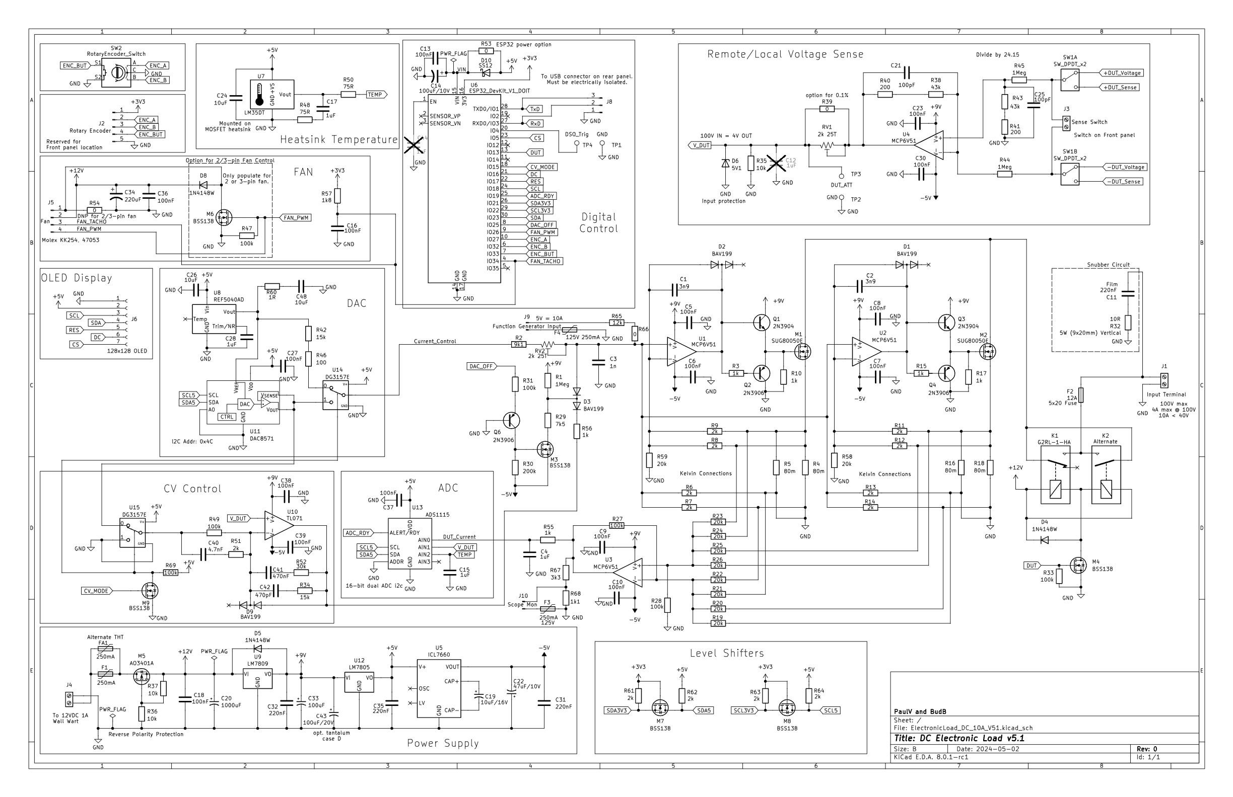
The first thing to notice is that there is a relay and fuse to protect the circuit guts against inadvertent stupidity. It's better to replace a fuse than toss an entire circuit in the trash. The nice things about relays are that they don't leak current when they're open and have decent contact resistance when closed. The system will power up with the relay open and it will be open with the power off, so if the user connects the load with reverse polarity it can be sensed, a warning issued and the the relay kept open until the reversed connection is removed. There are two relays to choose from: an expensive one ($20 --Paul's) and a cheap one ($1.5 -- Bud's). Unfortunately the two relays don't have the same PCB footprint.
The voltage and current feedback are from instrumentation amplifiers that are calibrated with a trim for accuracy. The current feedback amplifier's offset errors can be removed at system boot by measuring the zero current feedback voltage and subtracting it. The voltage feedback amplifier is a zero-drift chopper-stabilized opamp that should have very low offsets. This still leaves temperature drift as an error.
The current resolution is set by a 16-bit DAC with a range of 0-4.096V. Its reference is the REF5040. The DAC output is divided down to a full scale 0.2048V to the current loops controlling the current through two 40mR resistances, so the full scale current is 0.2048/0.02 = 10.24A, with a resolution of 0.15625mA/bit. It will take 64 DAC steps to make a 10mA step. Paul gets to do the math.
The voltage/current feedback resolution is set by a 16-bit ADC. The ADC has an internal voltage reference = 4.096V. Voltage resolution will be around 1.5mV/bit.
There are level shifters to compensate for the logic level differences between the ESP32 (3V3) and the ADC/DACs (5V) using the I2C bus.
We added a Function generator input (5V = 10A) to produce arbitrary waveforms. We also added a Current Monitoring capability -- a voltage output scaled to 1V = 10A, to see real-time current output on a scope.
Internal Power Supplies
We're using +9V, +5V and -5V for supplies. The ESP32 Devkit provides its own +3V3 as a source for logic level pullups. We would have preferred a +10V instead of the +9V, but the LM7810 doesn't have the headroom to do that. The opamps require +9V and -5V to drive the big NFETs. We needed the -5V to get to zero even with rail-rail opamps.
The -5V is generated from the +5V supply by a noisy ICL7660.
More later...