 Bud Bennett
I've seen some DIY articles that show the most basic topology for making a current source controlled by a voltage source. Here is a typical topology:
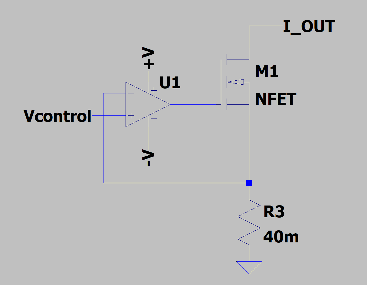
There is no compensation to prevent oscillation -- it assumes that the amplifier has infinite bandwidth and infinite gain. A more practical circuit might be this one:
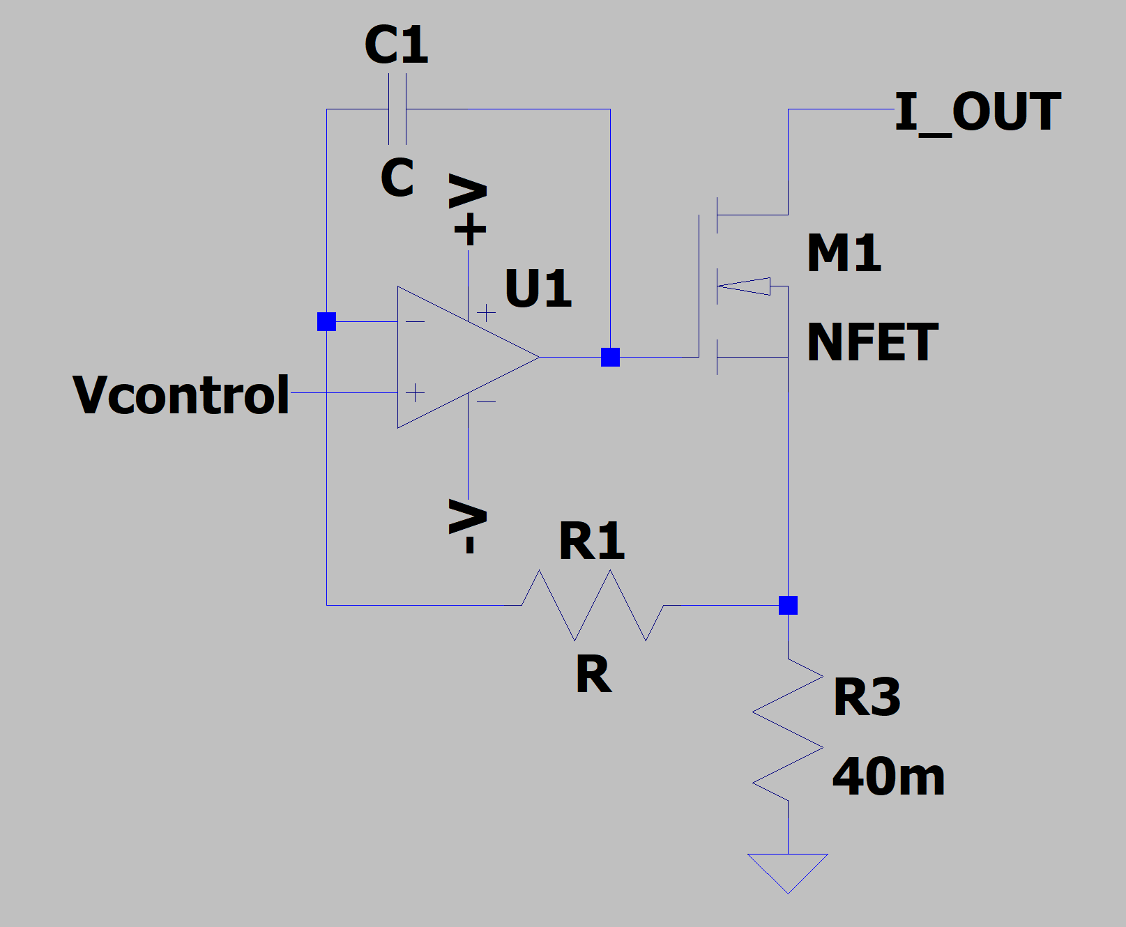
R1 and C1 create a "pole" that overrides the opamp's internal compensation to possibly prevent the circuit from oscillating. But this still neglects real world problems. Consider the circuit below:
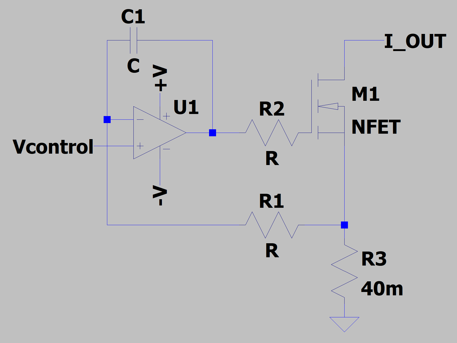
R2 is added because the gate capacitance of M1 is large (maybe 10nF), which causes the amplifier to become unstable and oscillate. Adding R2 "isolates" the amplifier from the capacitance of M1. R2 is typically 50-300 Ohms. Now we're getting close to something useable.
Our Approach at Present:
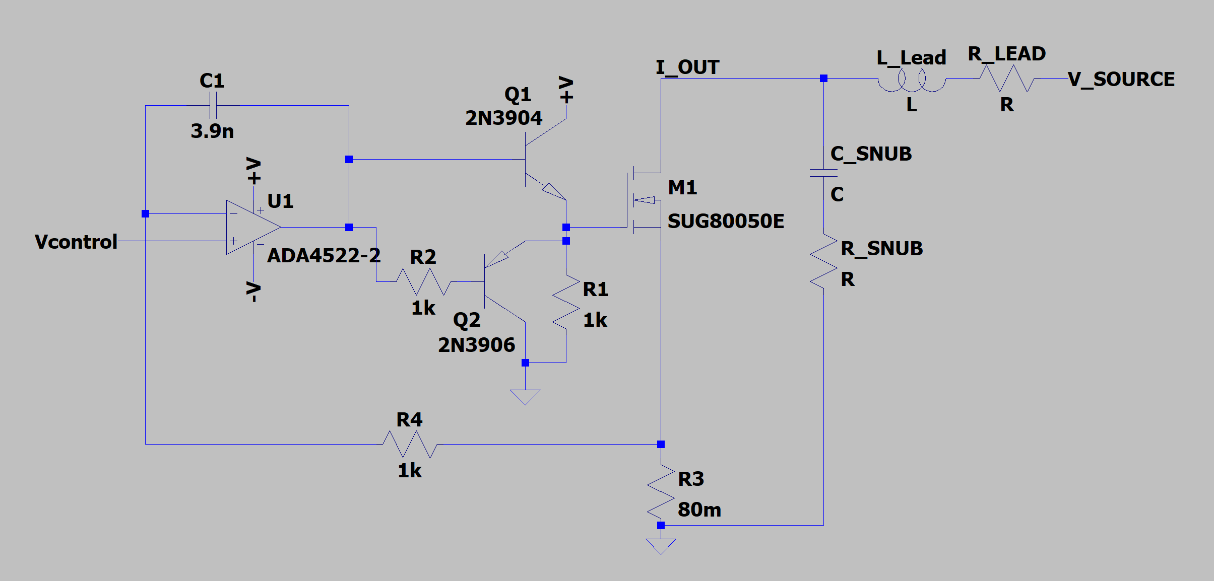
Oooh...lots more components. This schematic accounts for the inductance of the leads connecting the source to our load. The inductance of the leads makes a big difference in compensating the circuit to prevent oscillation. The values of R_Lead and R_LEAD vary with the length of the wires used to connect V_SOURCE to our load. Typical numbers for L_Lead and R_LEAD are 3uH and 100mR, respectively.
The addition of Q1 tends to isolate U1 from the gate capacitance of M1 and still provide plenty of current to drive the gate. Q2 doesn't do anything...yet. R4 and C1 create a unity-gain crossover that is low enough that the phase shift through the circuit doesn't reach 180 degrees to cause it to oscillate.
With R4xC1 having a short time constant (high frequency) the open loop response of the circuit would look something like this:
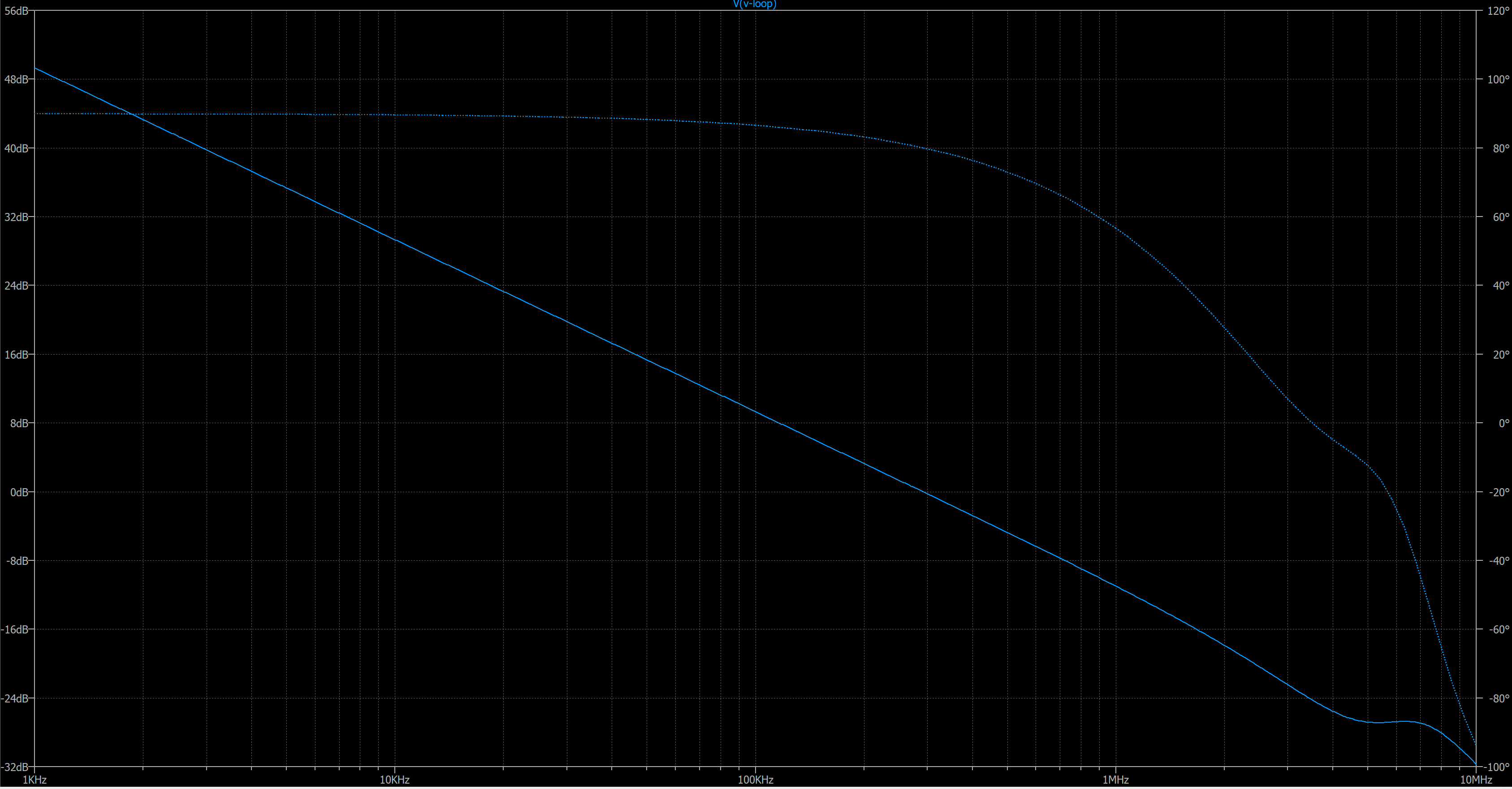
Note that the phase margin is nearly 90 degrees and the gain margin is 25 dB, indicating that the circuit is very stable and unlikely to oscillate. But what happens when we include the lead inductance?
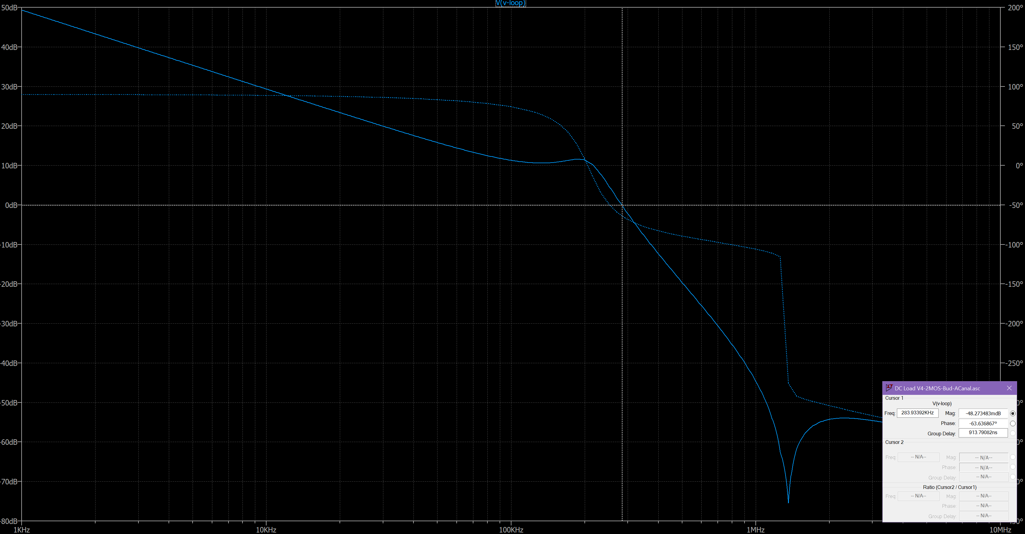
Now the phase and gain indicate that the circuit will oscillate about 283KHz. It's pretty ugly. It has to be taken into account in the design. The most straightforeward way to compensate for the lead inductance is to de-Q it so it doesn't create a large peak in voltage. That's where the snubber circuit comes in. If we add about 5 Ohms of resistance across the lead inductance it will reduce the Q of the resonant circuit and help prevent that oscillation. Here's what the open-loop response looks like with RSNUB=4.7 and CSNUB=1uF:
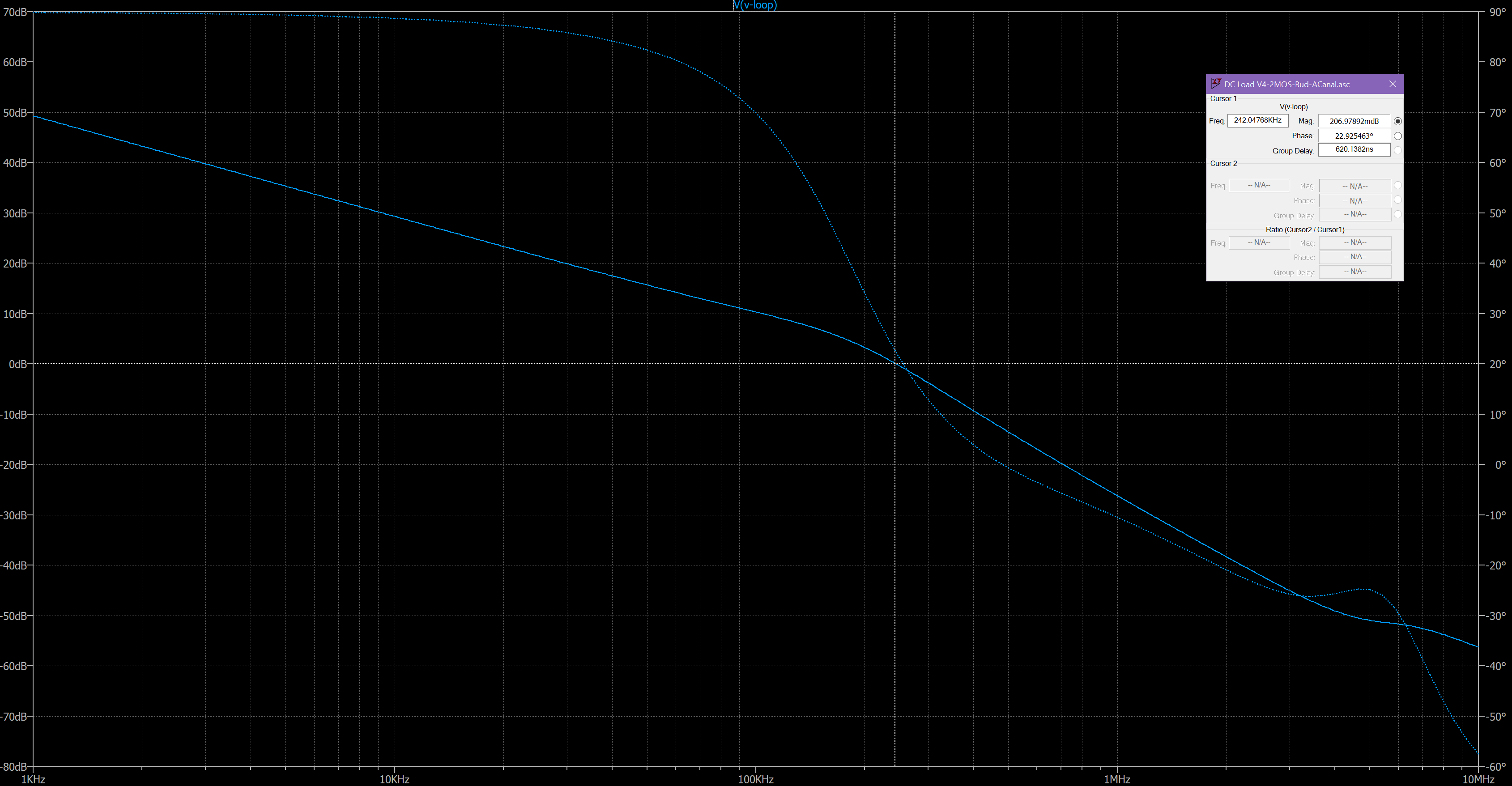
It's better, but the slope of the gain is too steep and the phase margin is only 23 degrees -- not good enough. Also notice that there is a peaking in the gain/phase response at 5MHz -- stay away from this. The easiest fix to increase the phase margin is to increase C1 until you get adequate phase margin. So increasing C1 from 300pF to 3.9nF gives us this:
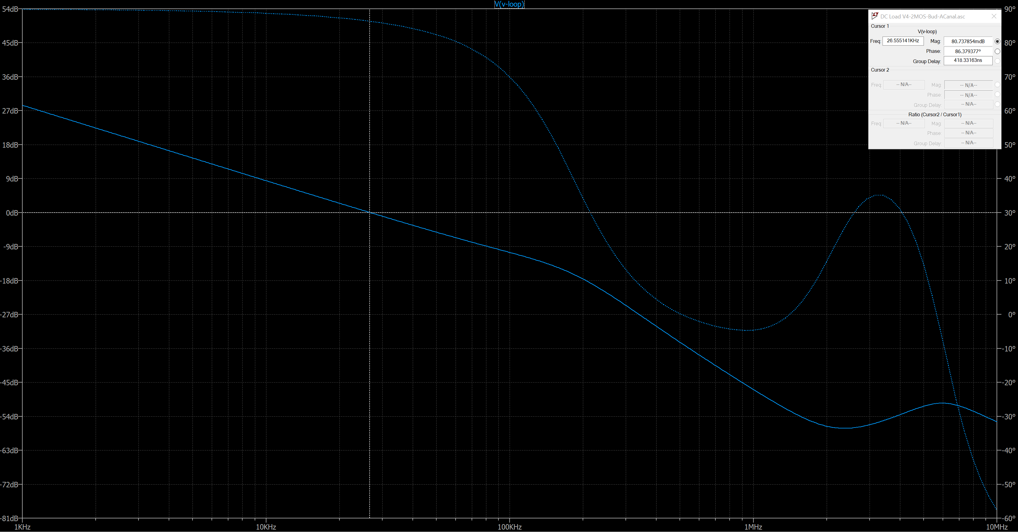
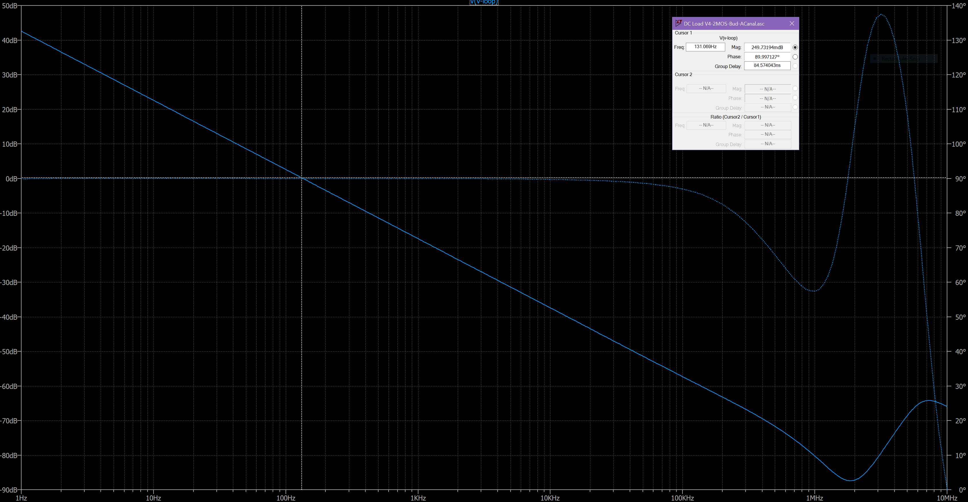
This looks even more problematic, but it's not. Note that the gain slope as it crosses through zero dB is only 20dB (very desirable for a stable amplifier). Note also that the phase margin has increased to 86 degrees and the gain margin is around 35dB. What we have given up is bandwidth since this loop only has a gain-bandwidth of around 25kHz. But that should be good enough for our purposes. We still need the snubber because without it the phase margin would still be near 90 degrees, but the gain margin degrades drastically to less than 10dB, which is marginal to prevent oscillation.
But wait...there's more. If we decrease the set point current from a high current to a very low current, say less than 25mA, the gain-bandwidth of the loop decreases to around 130Hz. This smaller than desired, but probably still usable.
So what are the other components for?
R1 provides current to decrease the emitter resistance of Q1 and also drive the gate toward GND. Q2 protects Q1 from a nasty transient that could damage it. And R2 limits the current into the base of Q2 if the opamp output goes below GND. More on that later...
Discussions
Become a Hackaday.io Member
Create an account to leave a comment. Already have an account? Log In.