 Bud Bennett
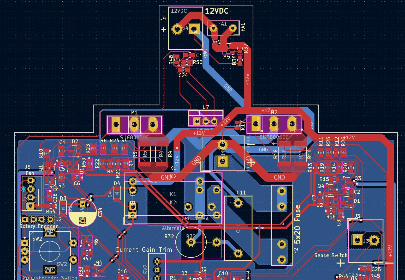
As of this date (2024-04-04) the PCB layout is frozen for this pass. I've been fiddling with it for several days -- making small changes that never seem to end. Here is the layout of the high current/high voltage section:
At the last minute we're specifying 1oz copper for this PCB. That change increased the traces carrying 10A blow up to 6mm width and the traces carrying 5A are now 2.5mm wide.
The GND reference
The first thing to notice is pin 2 of J1 (find it just below and to the right of U7) -- that is ground zero for the entire PCB. It is the absolute GND reference potential for the system. This is where the negative input lead of the load connects to the PCB. All of the various power inputs and outputs connect to this point. The 12VDC power adapter negative lead (in Blue) snakes around to the right and comes directly to that lead (a Kelvin connection). The top-side metal traces (in Red) that bring currents from the sense resistors, R4-R5 and R8-R16, are split equally/identically in terms of resistance, from those resistor's pads to J1 pin2. Those traces carry a maximum of 5A/each and are properly sized, by width (2.5mm), to carry that current without over heating.
The snubber capacitor, C11, also connects directly to the J1 pin2, but with a much smaller trace width since the currents should be smaller.
Lastly, the ground plane is almost a Kelvin connection but must share a small section of bottom-side metal trace. Hopefully, it will not matter much.
High Current Paths
The high current traces carry 10A max and require a trace width of 6mm. The input connector, J1, has a 6mm wide trace (in back-side metal, Blue) from it's positive terminal to the fuse, and also from the fuse to the relay (back-side metal, Blue), where the trace eventually splits and reduces to 2.5mm to handle the 5A currents to the drains of M1 and M2.
High Voltage and Creepage
The pads of the high voltage devices/connectors must have sufficient distance from other pads to prevent creepage. High potential between pads located close together can develop conductive "growths" that cause parasitic currents to flow and can eventually cause failure. This is not only a problem for exposed pads or traces that are not covered by the solder mask. The recommended pad separation distance to prevent creepage for a 100V potential is about 1.5mm. Traces located under a solder mask only need to be separated by 0.4mm to withstand 100VDC. The layout conforms to these restrictions.
Kelvin Connections
I'm assuming this technique is named after Lord Kelvin. Here is the layout detail on the left side:
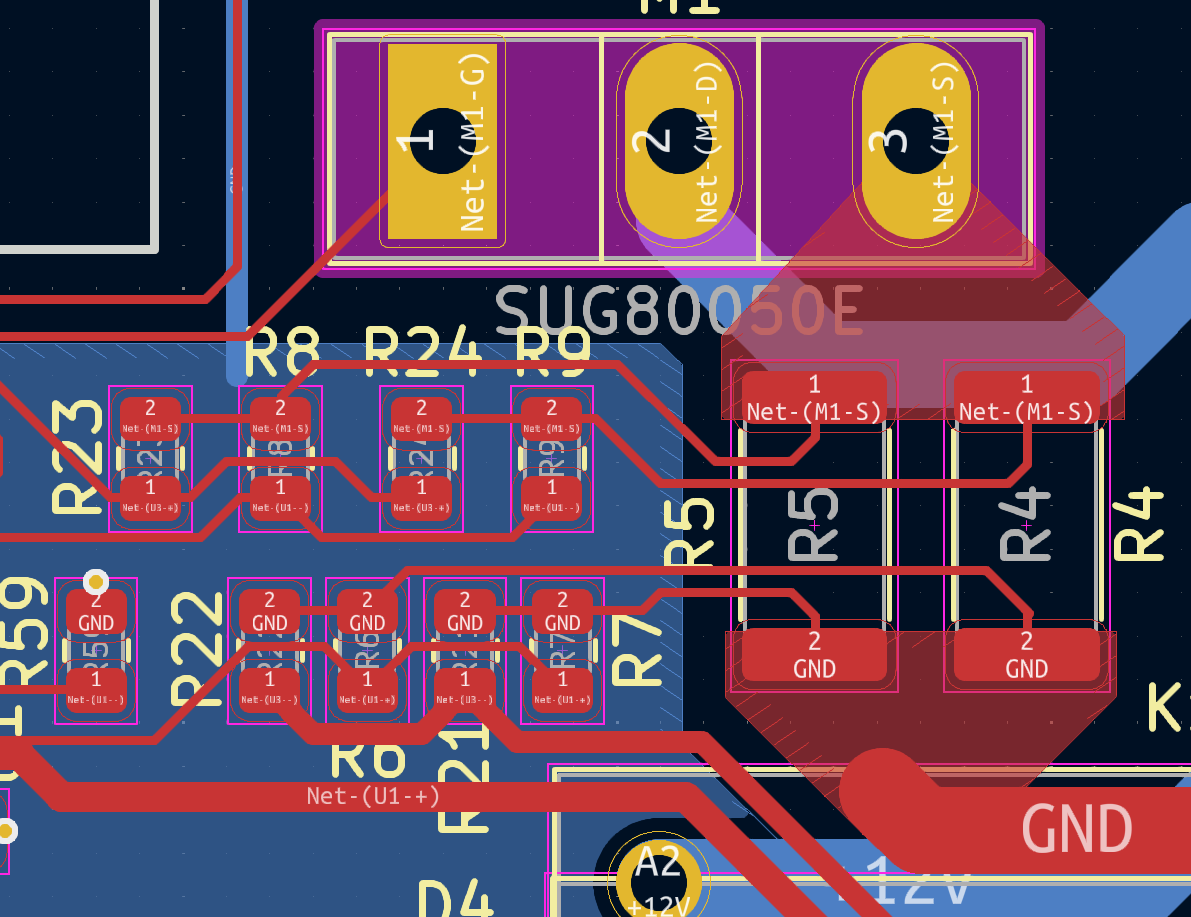 The current tends to spread in 45 degree funnels from a single point to a connection point, such as a pad on a component. In order to make the Kelvin connection the current should be zero at the point of the Kelvin connection. I made triangular copper pours to distribute the current to the two sense resistors. The back-side of the pads should have zero current flowing to it and therefore a good place for a Kelvin pickup. The pickup points are on the middle-inside of the pads on the sense resistors. Those traces connect the feed resistors for sensing the voltage across the sense resistors.
There is another method of picking off Kelvin connections from SMD devices, but this method was recommended by the manufacturer of the sense resistor...who am I to argue. We'll see how well this performs when we get the PCBs to evaluate.
Discussions
Become a Hackaday.io Member
Create an account to leave a comment. Already have an account? Log In.