 Bud Bennett
When the system boots up the relay should be open and the CC DAC should be set to zero. But this doesn't necessarily set the output current to zero. If the opamps controlling the current loops have a positive offset they will be unable to fix the current at zero. And if the offset is negative the opamp output output will drift to its negative supply if not constrained. Therefore, the only way to get zero current is to force it through some other means.
Dominik solved this problem by yanking the opamp input to a high voltage, which drive the output to its negative supply. This does enforce a zero current state at the output, but not without issues during normal operation.
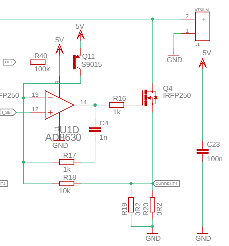
The leakage current from the collector of Q11 is not usually a term anybody cares about. In this case, the S9015 has ICBO=50nA, which is pretty low. This current generates an offset term across R18 equal to 0.5mV, or 5mA per opamp (and there are 4 of these, but not all will generate WC leakage current). In our case, it would create an output current error equal to 12.5mA.
The Keysight design just yanks downward on the opamp output, forcing the opamp to output short circuit current. This is bad because the opamp generates a relatively large output current, but is good because any error current from the downward yanking device gets swallowed by the opamp in normal operation and doesn't impact performance.
Both of the approaches above force the opamp into a state of inequality. The output is driven to a rail and the inputs aren't equal. When the opamp is released from this condition there is usually a transient spike of uncontrolled magnitude until the conditions of equilibrium are re-established. Generally not good.
Our Approach
We chose a different path.
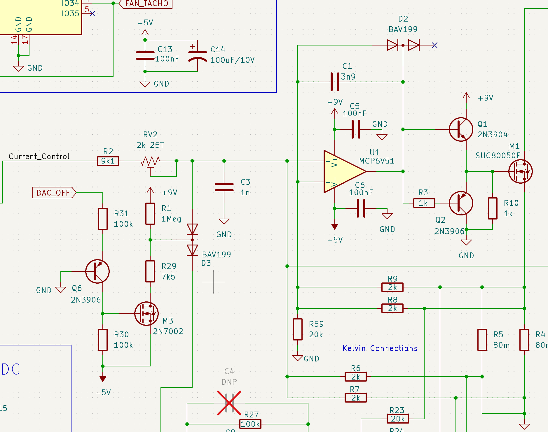
The BAV199 low leakage diodes are actually specified over temperature and voltage! They're spec'd at a max reverse leakage of 5nA at 25C, and 80nA at 150C. The datasheet even provides data for typical and max leakage current as a function of temperature: 3pA typical at 25C, 300pA typical at 100C, 5nA max at 25C and 30nA max at 100C.
In normal operation D3 leaks current into the "+" input of the two opamps controlling the current loops, getting absorbed by the 500R equivalent resistor at that input. But this is partially compensated by a reversed biased D2 leaking current into the "-" input of opamp U1 (and D1 leaking into U2), getting absorbed by the 1k resistance at those inputs. The currents are not going to match, so we can use typical vs worst case to see what the range of error might be. But the difference between typical and WC is so large that the typical value can be set to zero. If D2 is leaking worst case then it will produce an output current error equal to -(30nA x 1k)/0.04R = -750uA. If D3 is the WC condition then it will produce an error current equal to +(30nA x 500)/.02R = +750uA. So it seems the error current will drift somewhere between +750uA and -750uA WC as the box heats from 25C to 100C. If we use just typical numbers then the offset error drift is only -7.5uA. That's manageable.
How it works
Normally, the DAC_OFF signal is low (zero volts). Therefore Q6 and M3 are "off" and the BAV199 diode, D3, is reversed biased and not influencing the current loop significantly. If the DAC_OFF signal is asserted to 5V then Q6 drives the gate of M3 to a VGS ~ 4V and M3 switches "ON", which then pulls its drain to -5V. R29 then forward biases the upper diode of D3 and pulls the "+" input of U1 below ground. The amount of negative voltage at the "+" input of U1 depends upon what the DAC value is. If we assume the DAC is outputting 4.096V or less, then the opamp "+" input is yanked below GND. Since the gate of M1 can't go below GND the opamp output will drop, forward biasing D2 until the opamp inputs equalize...somewhere around -1V. R3 is there to limit the current into the base of Q2. So now the gate of M1 is at GND and there is just leakage current flowing through the NFET.
When DAC_OFF is de-asserted, D3 is reversed biased and the opamp is freed to do what it wants. Since its output was held below GND while DAC_OFF was asserted, now the output is released and allowed to increase, at the rate determined by C1 and R8//R9 -- slowly if the CC DAC output is set slightly above zero. This could take tens of ms if the DAC value is low.
There is no big current spike at the output when DAC_OFF is de-asserted.
Discussions
Become a Hackaday.io Member
Create an account to leave a comment. Already have an account? Log In.