 zst123
Introduction
This clock has great sentimental value to me from my childhood as I grew up with it. Unfortunately, the clock accuracy started drifting severely. I have to set the time daily as it goes out-of-sync up to 10 minutes each day.
Many nostalgic things to like about this clock. It has an FM radio which I listened to daily as a kid. I always loved how it looked ahead of its time with the large digital font. Growing up, this clock piqued my interest in the rising field of digital electronics.
In this project, I will share my journey to retrofit it to give it a new life. Here I shall automate it to synchronize to internet time periodically.
Teardown
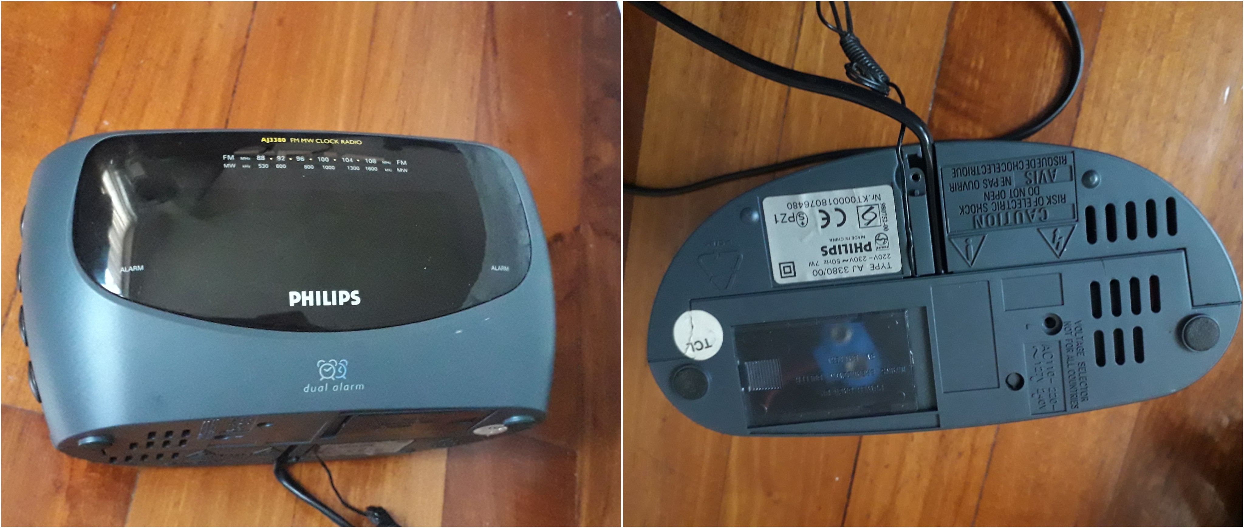
Let's tear down the device to understand how it works. Firstly, the model is a Philips AJ 3380/00 Digital Radio Clock. After unscrewing, we immediately see the large components such as the speaker, AC transformer, seven segment display and mechanical buttons.
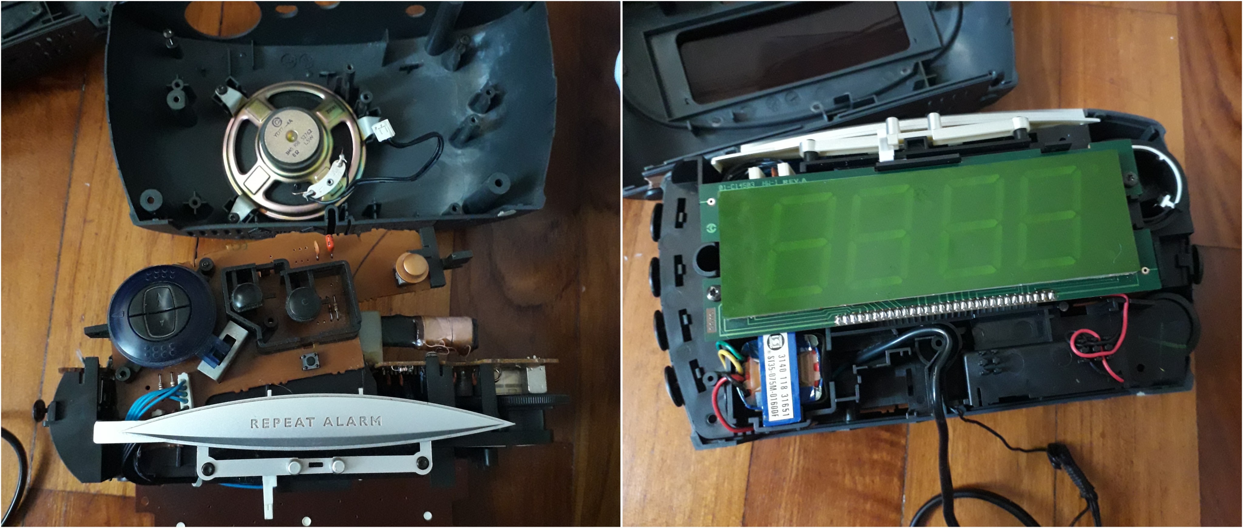
I continued disassembling it until the main circuit board. At this point, I stopped tearing it down further as the circuit board was secured quite tightly with the plastic clips. Nevertheless we have enough information to plan the possible points of modification.

We see that the circuit board is dated March 1999. (Just about my age!). We also know that the clock IC controller is a LM8562. The circuit board matches very closely to the application circuit in the LM8562 datasheet.
Points of modification
The goal is to automate time synchronization. We can use a microcontroller to do the following:
- read the current time, and
- adjust the time
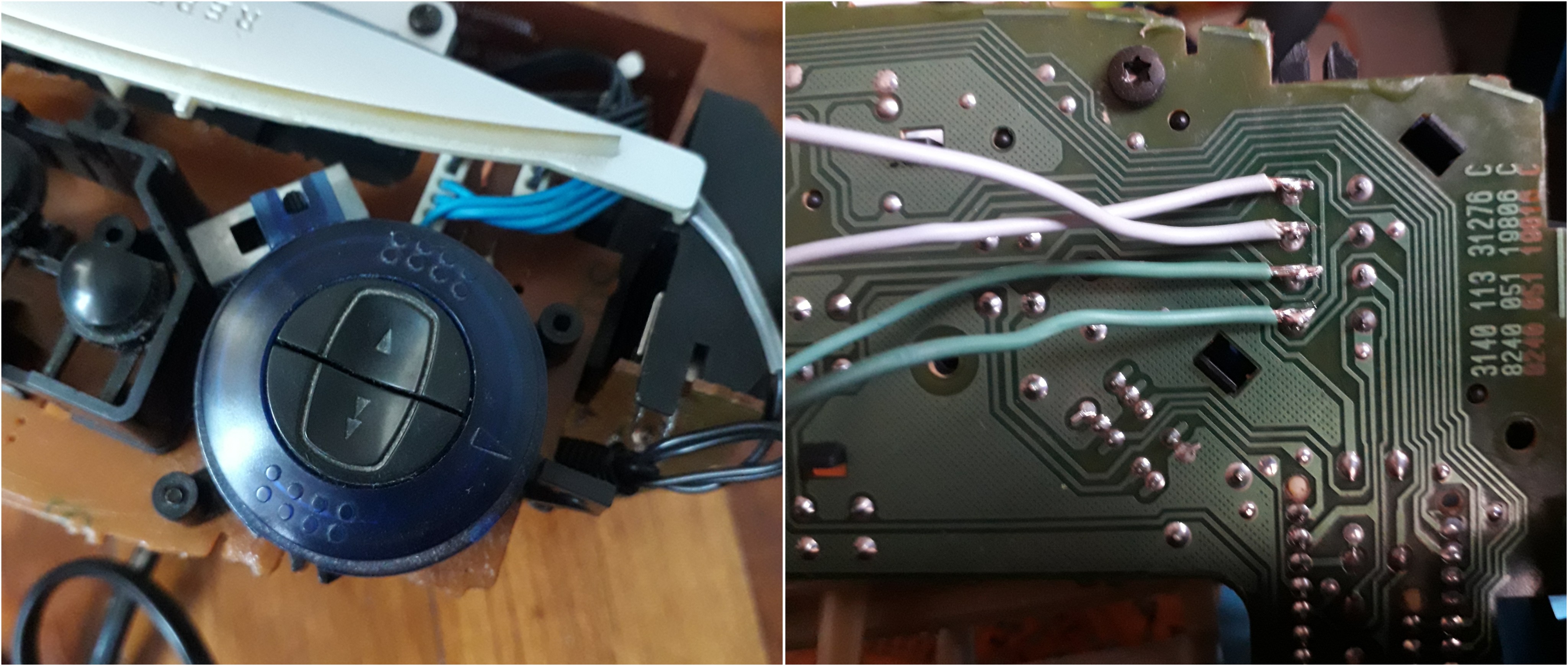
To adjust the time, the clock provides two buttons: Up and Down. I soldered some wires here to access it later.
An analog switch IC can be used to simulate the button press.
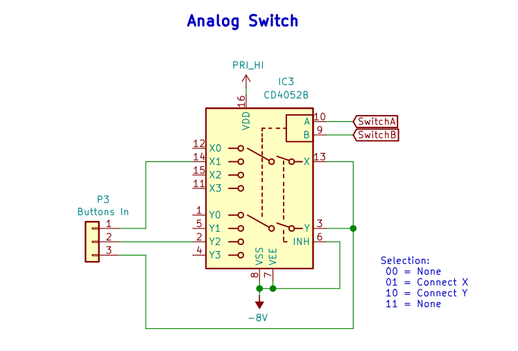
However for reading the current time, it is slightly complex. The only way I can think of is to read it off the seven segment outputs. Also be aware that there is display multiplexing involved.
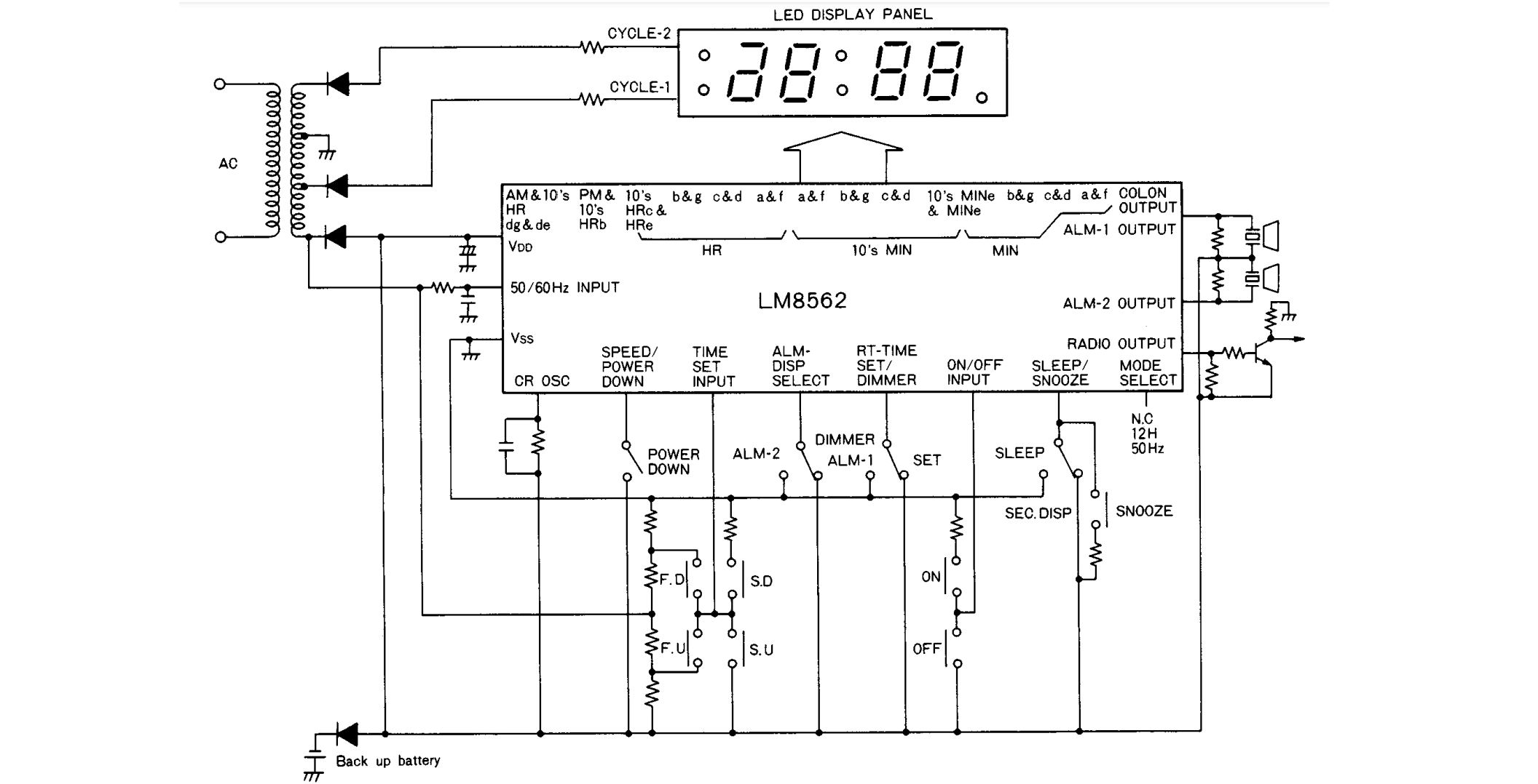
Understanding LM8562 display multiplexing
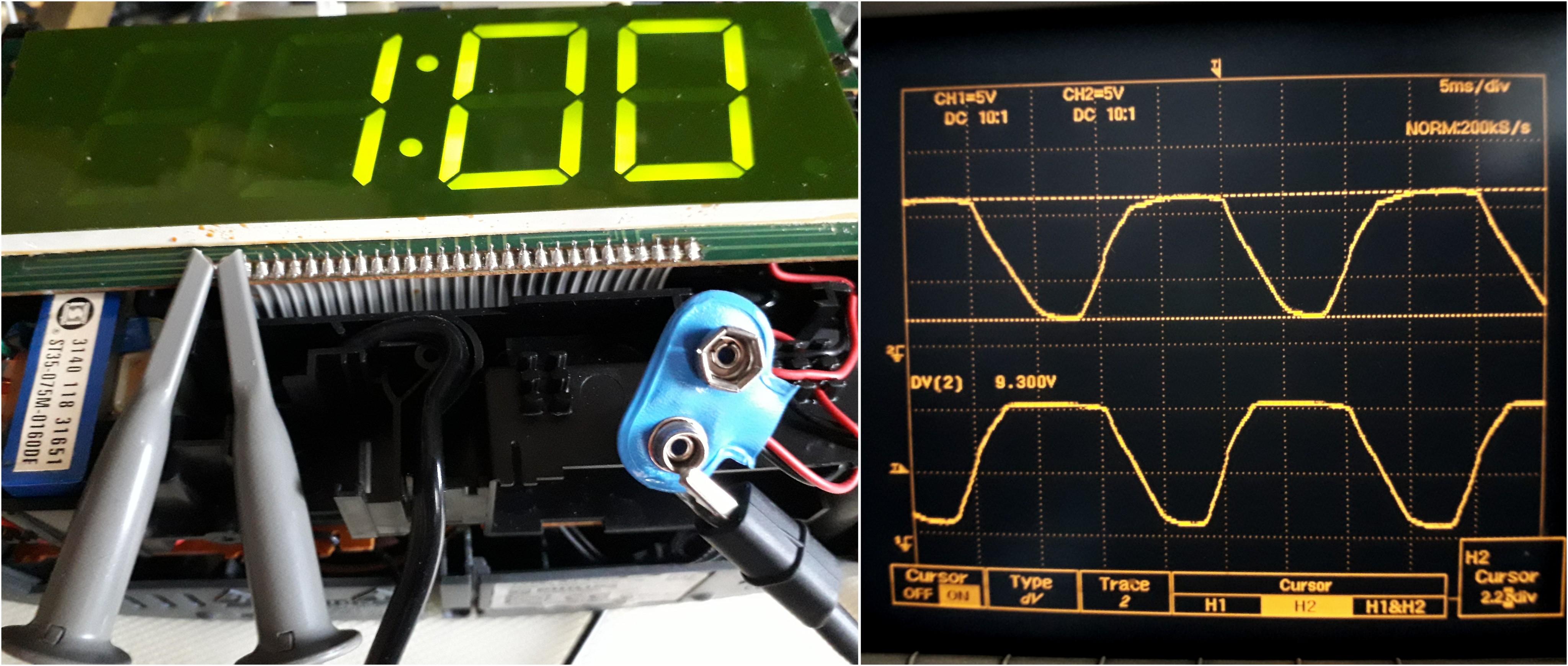
From the LM8562 datasheet, we also see the sample application schematic. From the schematic, the display is driven by two cycles of multiplexing. AC voltage directly from the transformer is used for display multiplexing.
I probed the supply pins of the display with an oscilloscope. This is the complementary 9V peak-peak 50Hz sine waves used for multiplexing. (Note: my grid supply is 50Hz where I live).
[Danger!] AC voltage is involved. Oscilloscope grounding must be done with care. From the schematic, the ground is referenced to the negative terminal of the battery. Hence I attached the oscilloscope ground clip to the battery connector.
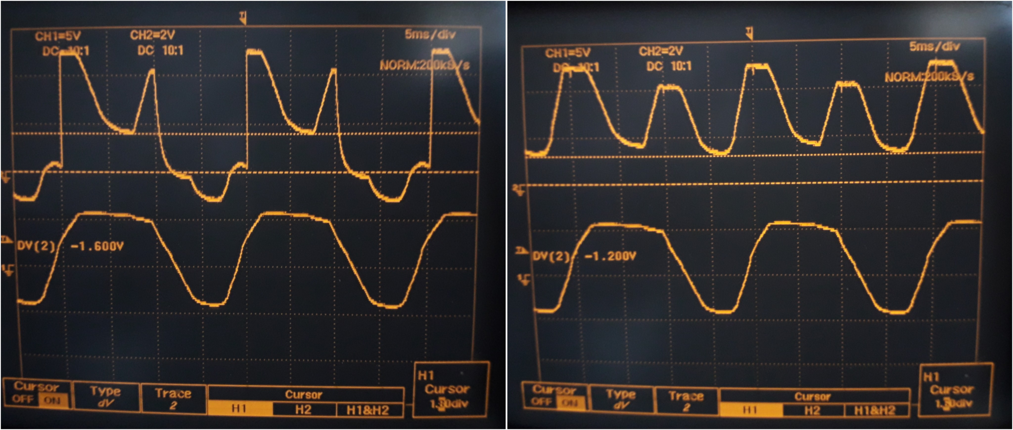
 The waveform on the segment pins resembles a rectified sine wave (double the frequency at 100 Hz).
 - On the left image, we see a segment lit up for only one segment (one multiplex-cycle is negative below GND and the other is above GND).
- On the right image, we see a segment lit up for both multiplex-cycles (the entire waveform is above GND).
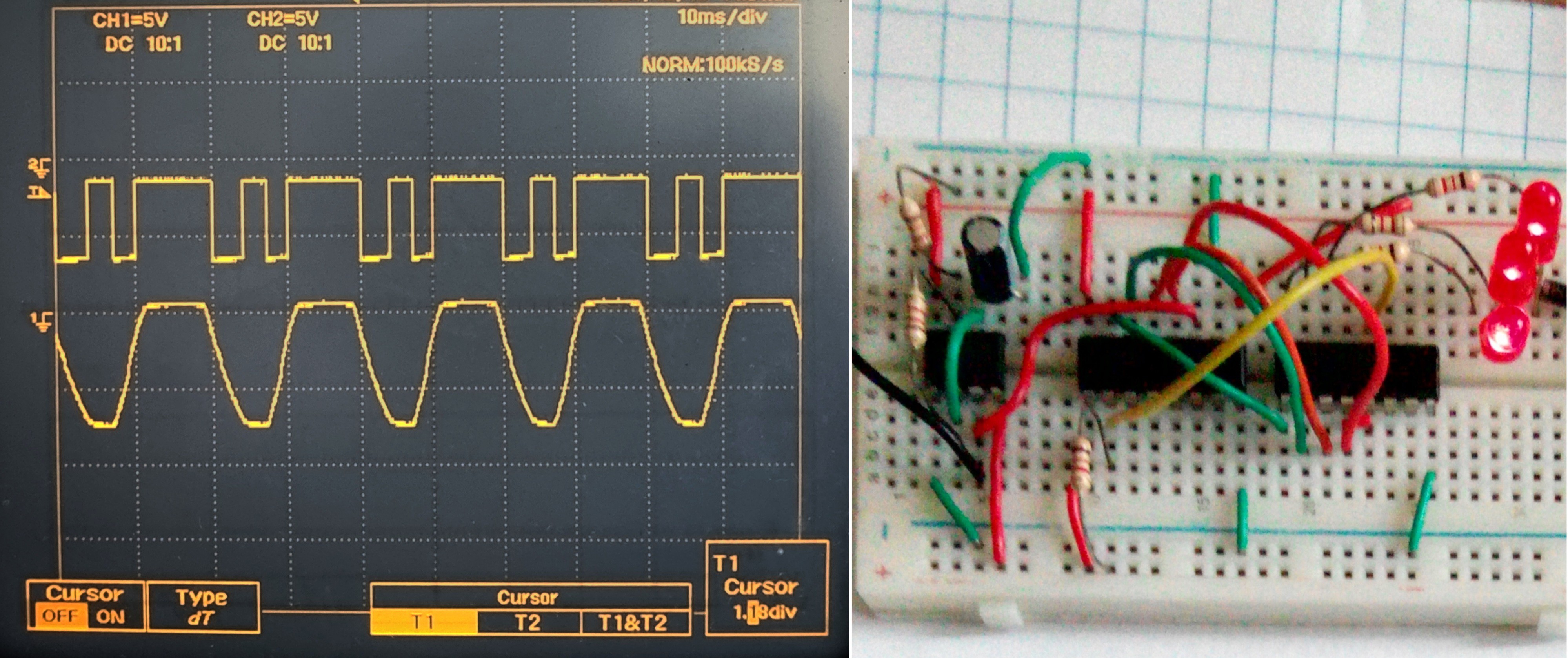
Using a simple opamp comparator, I can detect which phase (of the two multiplexing cycles) it is in, and also whether a segment is lighted up (High/Low). I also added an optocoupler as a convenient way to do level shifting (between the 9V analog to the 3V3 digital microcontroller).
Reverse Engineering Display Pinout
Now all that is left is to find out which pins correspond to which segment.
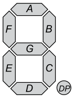
I shorted each pin to GND to determine which of it belongs to which segment. A lighted segment will turn off when shorted to GND.
After all the reverse engineering, I came up with the following pinout.
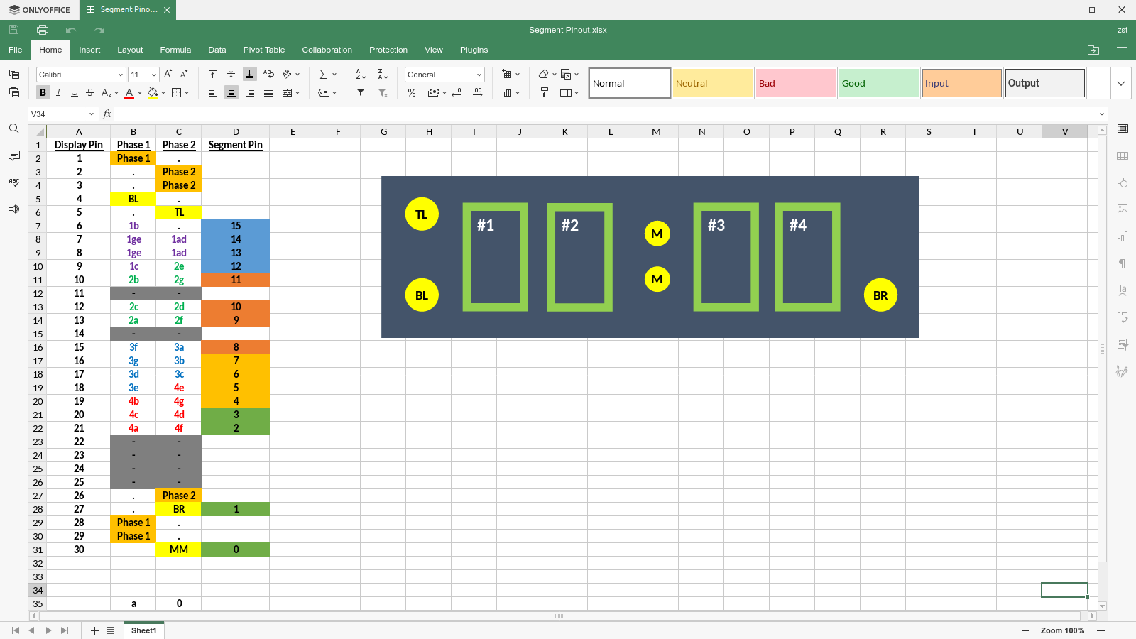 Finally, I soldered wires to breakout the display onto a connector of 16 wires.
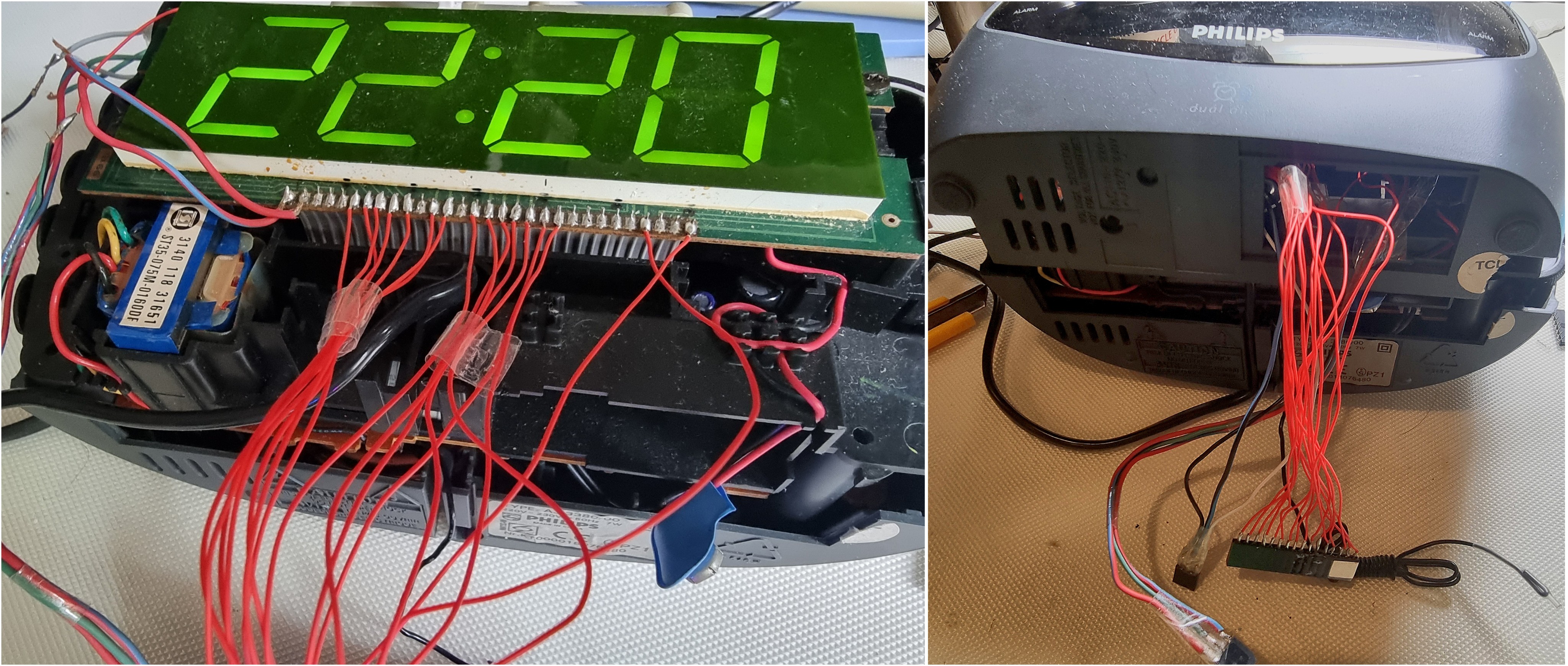
PCB Design Circuit
Putting it all together, I designed a PCB with the following major items:
- WiFi-enabled ESP8266 module was chosen as the microcontroller.
- MCP23017 I/O Port Expander to read all the 16 input pins of the connector....


 goldenshuttle
 mircemk
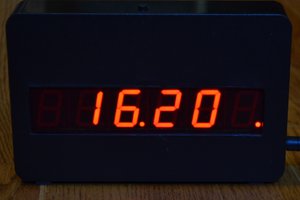
 Gigawatts
Hmm, since your clock gets its timing from the 50 Hz mains and you appear to be living in a first world country, you should have pretty good accuracy in the long term. It sounds like you're losing cycles from the mains. It might be the RC filter on the frequency input pin. If all else fails, you can buy LM8652s. Of course then you'd have no excuse to hack. 😉