After I broke some PCBs I started to get the idea what should be done to increase probability for successful PCB print
So one thing we can notice is the trace width. If wide trace is used fine details cannot be printed.
Let's see three different traces: over etched, under etched and one just the right width.
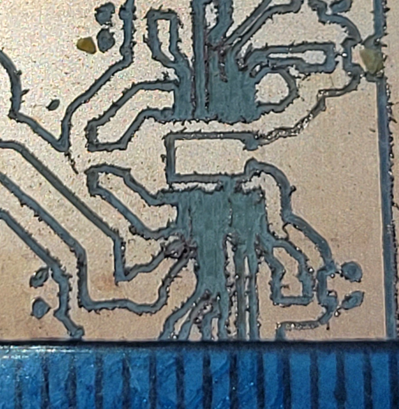
Here is example of 0.5mm chip layout, it's totally erased. Let's take a look at it under the microscope
The width is 0.35mm.
Now let's look on one which is has very fine details
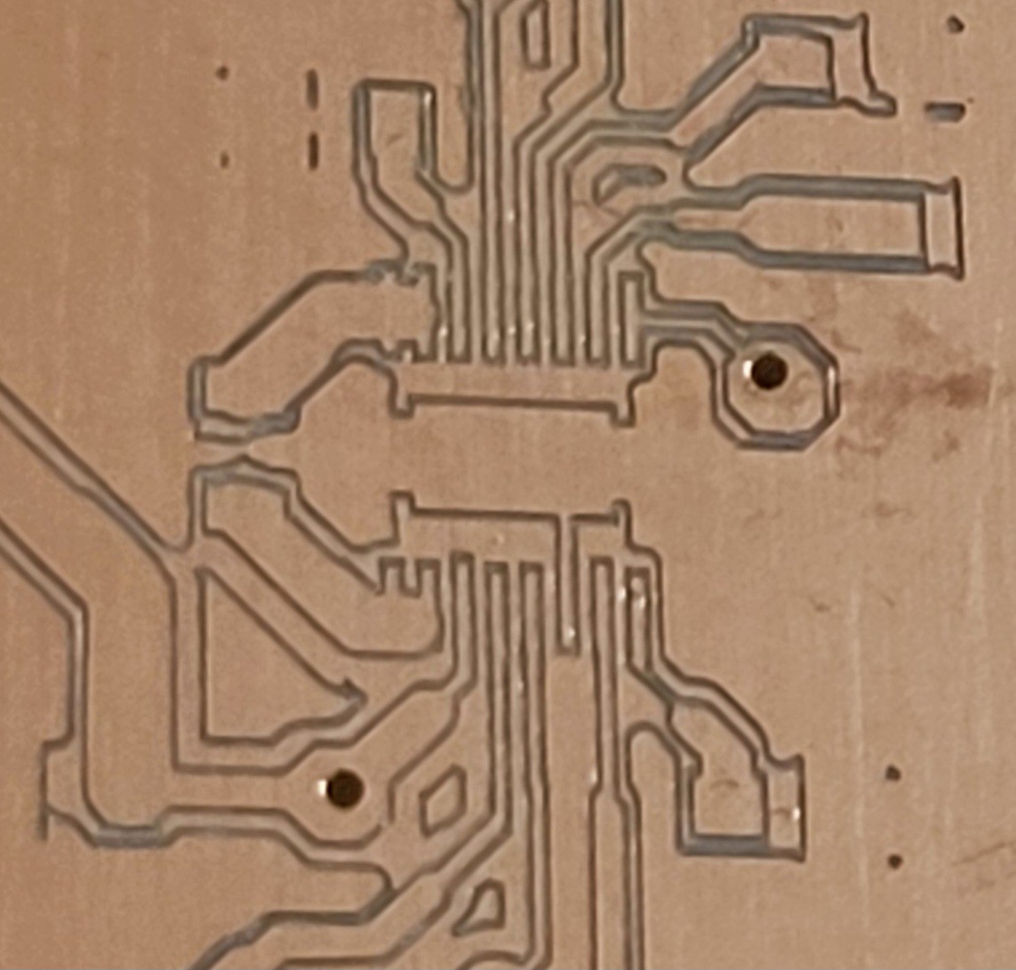
Now let's take a look on under etched one
It's width is 0.2mm.
Here is another one with just the right width
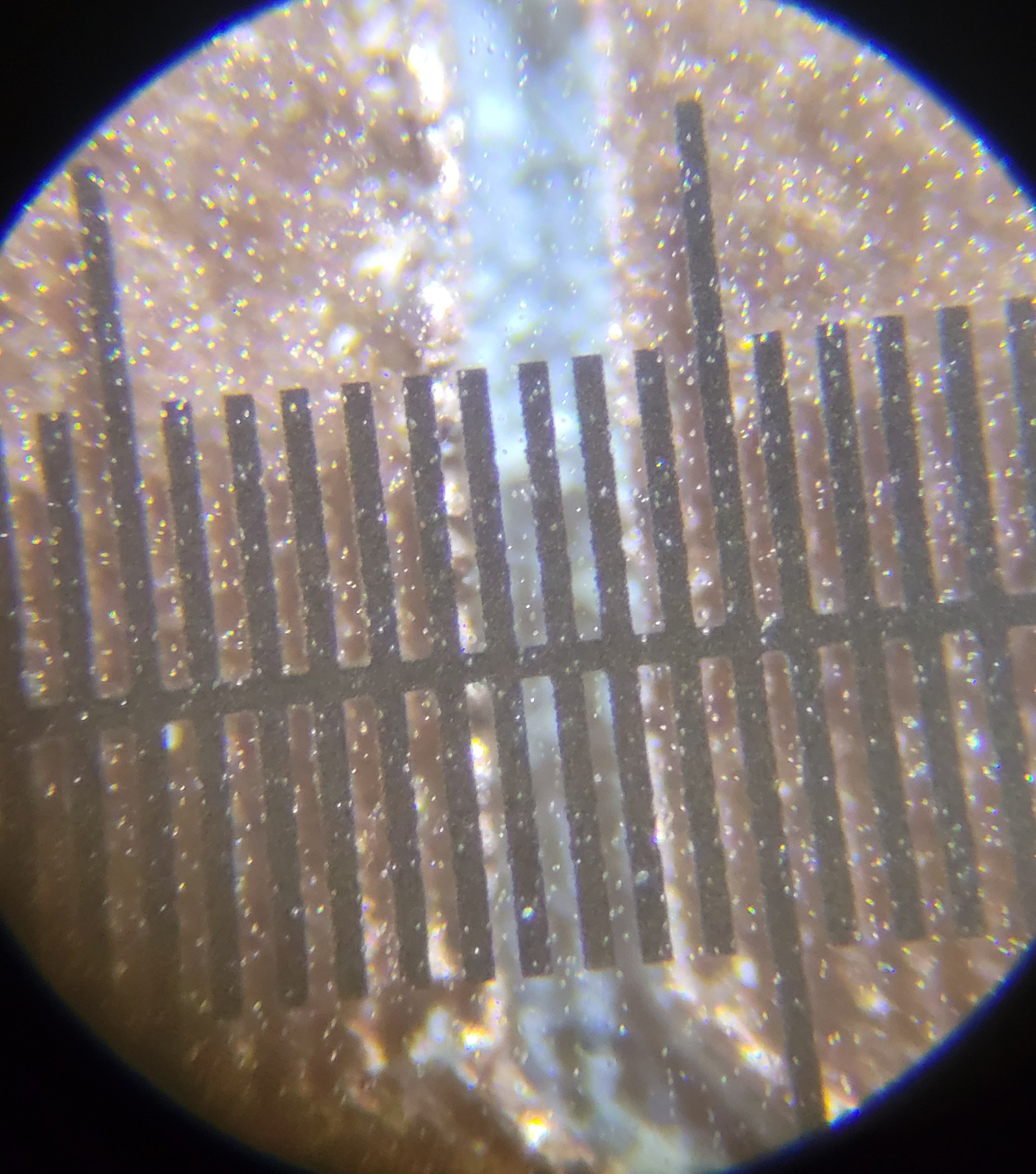
This time it about 0.25mm
So what is the difference? The only thing was changed are the bits and the copper plate.
It's possible that plates have different thickness of the copper.
But what about the bits are they same?
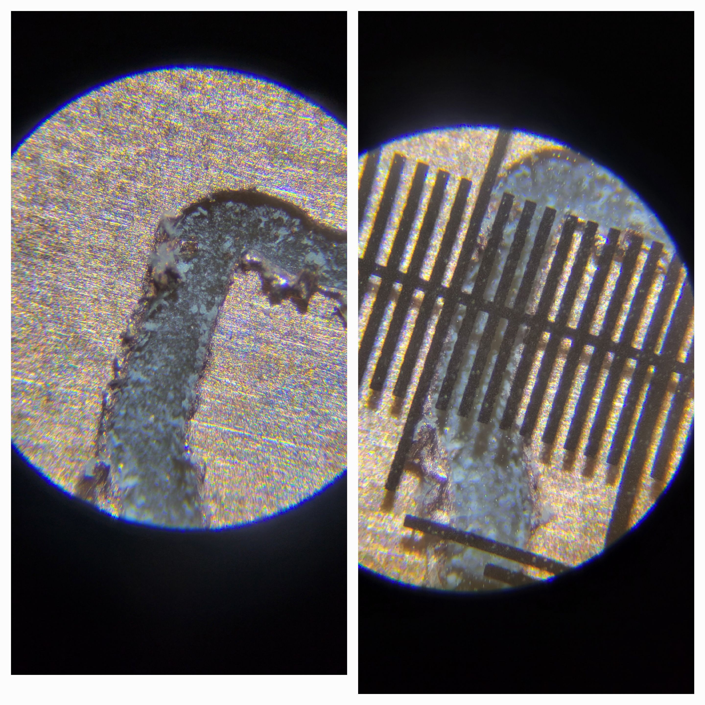
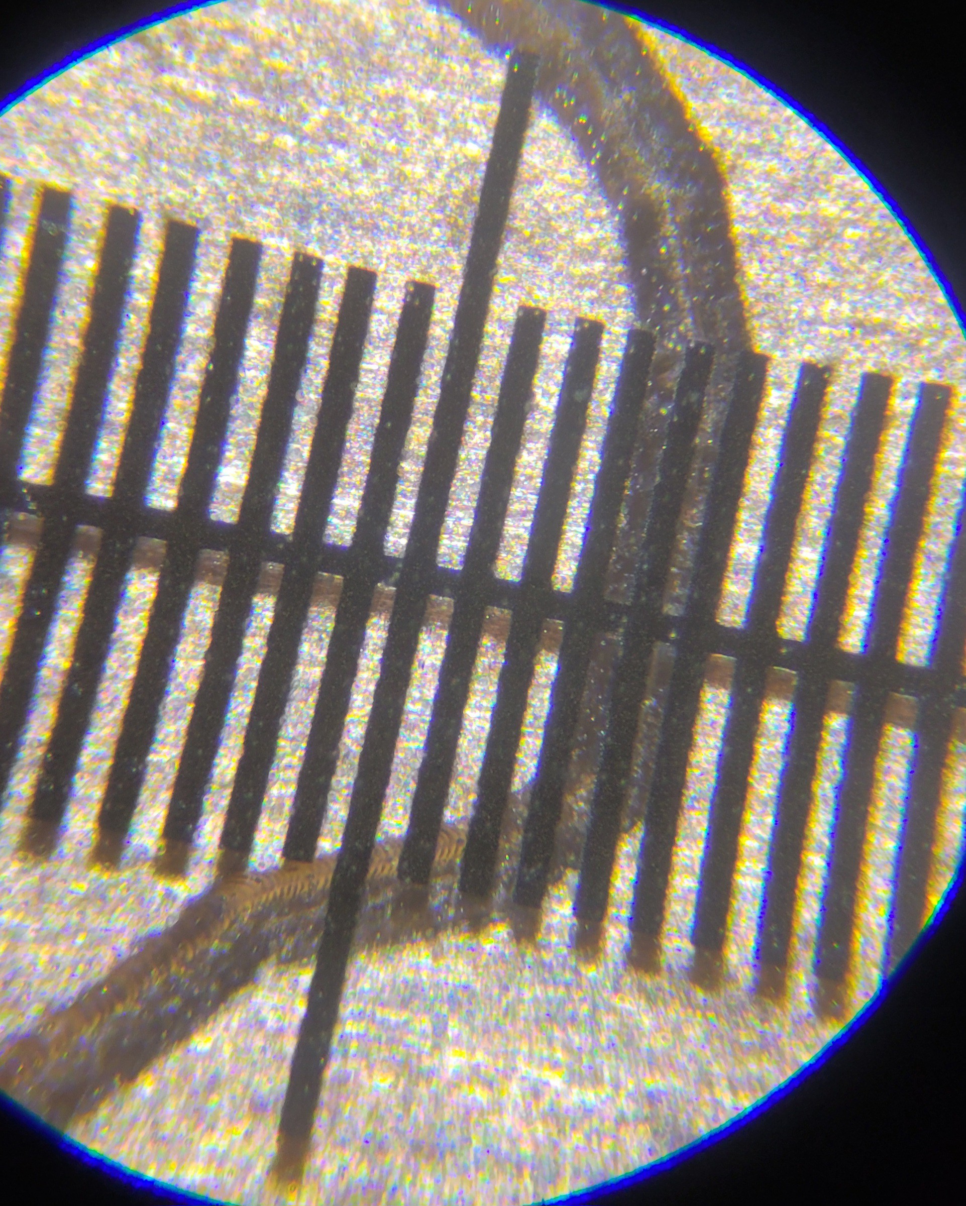
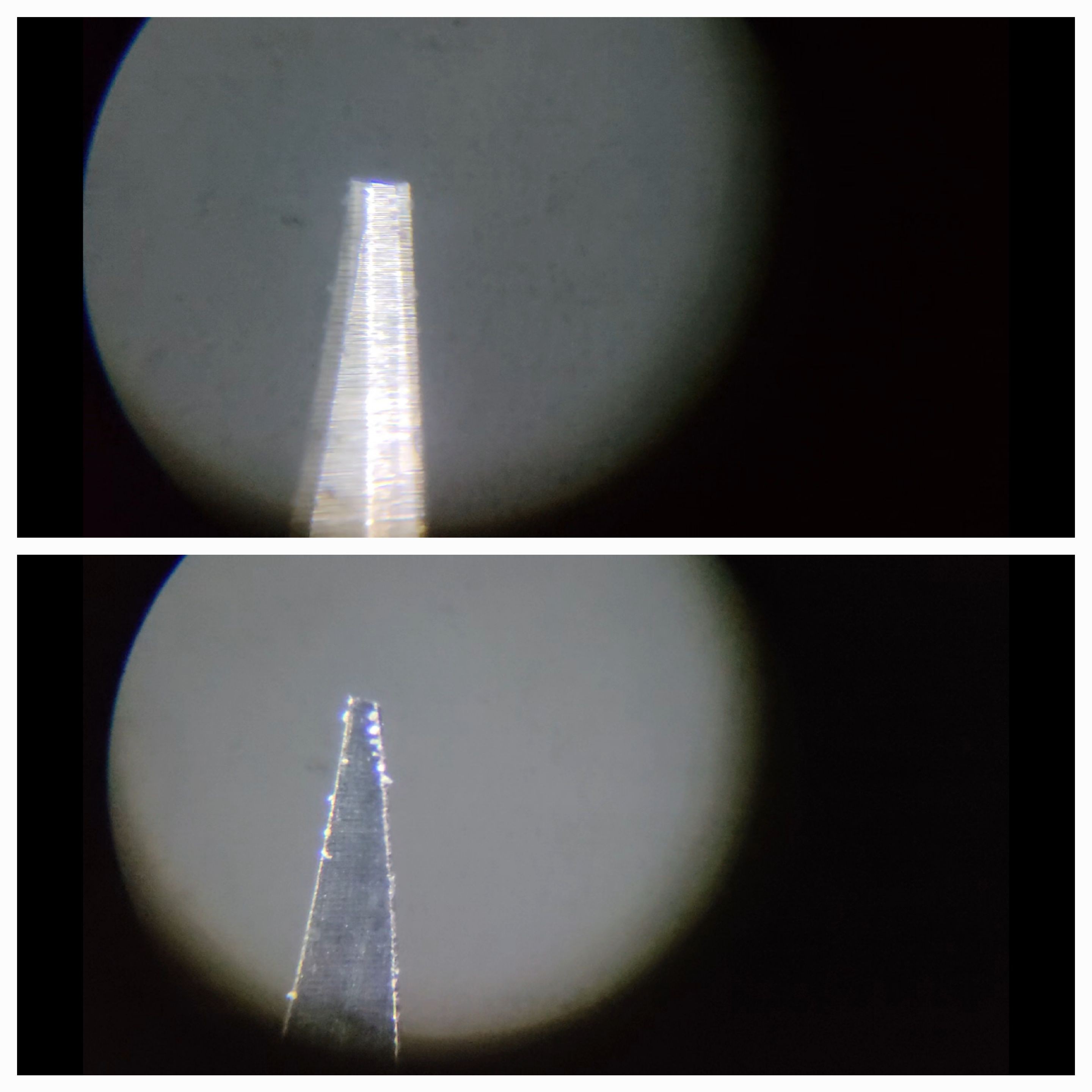
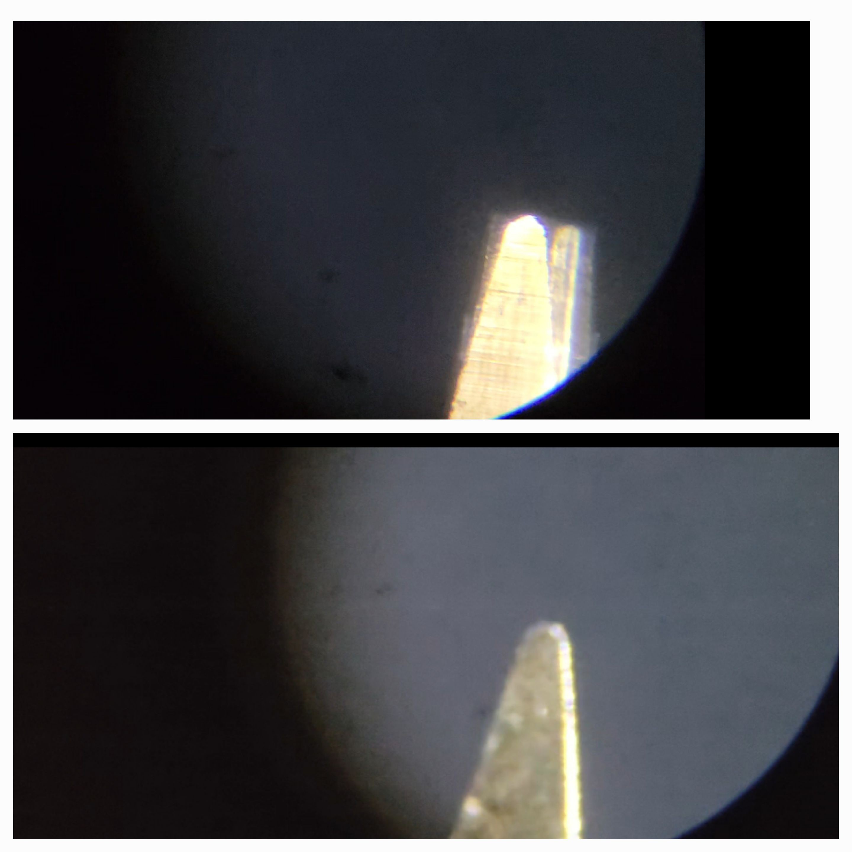
Let's take a look on the bits under the microscope.
Compare the tip statically and once rotated
The good: (upper part is rotating and lower is static)
The bad: (upper part is rotating and lower is static)
The main problem with milling is setup. Even if you run height map of 5mm steps, you will have still the problem that each bit has it's own depth configuration. Since sharpness and movement of the tip is greatly changes between different tips of the same company of the same batch.
Discussions
Become a Hackaday.io Member
Create an account to leave a comment. Already have an account? Log In.