 ridion3D
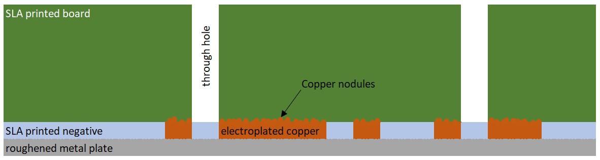
Disclaimer:
I abandoned this project over a year ago because of ADHD, anxiety and self-doubt. I'm only posting it now because I saw a post on reddit a few days ago that described what I'd done a year ago, and it made me feel sick that I hadn't published it then because I thought it was useless.
I haven't really documented anything back then, so everything I write here is from memory. And sorry if there's too much information, it was quite therapeutic for me to write it all down.
Start:
Over a year ago now, I needed a very simple PCB for a very simple project, but it had some surface mount components, so one of those through-hole prototyping PCBs wouldn't do. I could have etched a plain copper PCB the usual way, but I hate cutting and drilling them with a passion.
Since I had an FDM 3D printer, I thought I might be able to print a plate with channels for thin wires and then solder the components to the wires (pretty much like so: reddit). After a few attempts, I abandoned the idea because the heat from the soldering iron would damage the plastic.
The next thing I thought of was printing a board with the through-holes, then glueing a sheet of copper to it and doing the normal dry film, exposure, development and etching process. I also used a laser printer to print directly onto the copper, so I didn't need the dry film, which worked better than expected, but not that great.
This is one of the few images I have of an FDM printed board. It seems to be one of my earliest attempts. I think it was one where I laser-printed directly onto the copper, because of the black parts and the bad quality of the etching. Also aligning the copper with the toner transfered layout onto the plasic was hard.

Although it worked somehow, as my 3D printer obviously couldn't produce consistently good small holes, it ended up being more work than if I'd just drilled a normal PCB. It also had some other problems I can't remember. I printed it upright on one side instead of flat to get nicer holes, so it would also be prone to breaking along the layer lines.
I was then in this ultra-motivated phase where I really wanted to make it work. So I bought an SLA printer, thinking it should be able to print a perfect board with nice holes.
Since I had no experience with resin printing at all, it took a while and almost a bottle of resin to get a feel for it. It's pretty straightforward when you're printing larger things, but it's a bit trickier when you're printing holes as small as 0.6mm. Then bleeding and whatnot comes into play. Also the first layers need a longer exposure time to stick to the build plate, but this will make the holes smaller or close them completely.
It took a lot of time (and resin) to get consistently good results, but I was reasonably happy with it.
Copper Layer

My initial idea was to print the board with the through-holes directly onto a sheet of copper and then do the standard dry film stuff. So I ordered a roll of copper tape. It was a bit thin, but for simple prototype digital circuits it should be enough, I thought.
So I stuck a piece of the copper tape onto the stock build plate of my printer and tried to print the board onto it. As you can imagine, the resin didn't stick. I tried to make the copper surface rougher by sanding it. But it just didn't work. The sandpaper was either too coarse, so the thin copper would tear, or it just didn't do anything to the copper. The soft glue under the copper made it difficult. So I scrapped it.
The next idea was to just glue the copper onto the board like I did with the FDM printed PCB. I used some generic 5 minute epoxy glue. But here I had a similar problem. The copper wouldn't stick to the epoxy. Again I think because it was too smooth. I went through with the dry film and so on, and visually it looked great, like a real PCB, but it was far too easy to peel the tracks and pads off.
Soldering didn't work either. As the resin and epoxy were not designed for high temperatures, it's no wonder. So I ordered high-temp resin. As it had different printing characteristics to the resins I had used before, I had to go through the whole testing process again to get a good print.
Then I concentrated on the epoxy. It was a two component epoxy and I measured it by eye to this point. So I bought a fine scale. The results got better, but not good enough. (At this time I had heard the name JB-Weld, but I thought it was just a "normal" 2-component-glue).
So if printing directly onto the copper didn't work because the resin wouldn't stick, and glueing the copper onto the board didn't work either (it does, but not with the epoxy I had at the time), then maybe making the tracks and pads first and then printing the board onto them might work. The resin could stick to the build plate between the tracks etc.
I had two ideas on how to make the copper tracks and pads. Not the first idea I had, but the first I tried, was to put the copper tape on the build plate, put the dry resist on the copper, expose, develop and etch. Then remove the remaining glue from the copper tape with acetone. This kind of worked, but the acetone got under the thinner tracks and pads and lifted them off, too.
Remember that printing directly onto the copper didn't work because the resin wouldn't stick to the copper. So why would it stick to the copper tracks now? Well, my thought was that maybe the resin just didn't stick well to the copper because the exposure time was so short (it had to be, otherwise all the little holes would be closed by bleeding). And if I exposed it to a lot of UV after printing, it might stick to the copper quite well. Also, the resin would "hug" the copper tracks on the sides and hold them even better, I thought.
Okay, well. The whole process was not that great and I just kept trying because I can be stubborn.
Electroplating
The other idea I had was to electroplate the copper. Many years ago I wanted to make plated through-holes at home and had experimented with copper plating, so I already had a recipe and some equipment. So how do I get the copper to deposit only where I want it to on the build plate? One way would have been to put dry film on the build plate, expose it, develop it and then put it in the electroplating bath. But my initial goal was to reduce the process to as few steps as possible. Since I already have the SLA printer, why not print a thin layer of the negative of the curcuit layout onto the build plate with resin and place it in the electroplating bath?
One of the first things I did after getting the SLA printer was to see if the resin could be used as an etching resist. Instead of the dry film. So I put some resin on a bare copper PCB, put a thin clear plastic film on top, exposed it, rinsed it, cured it and then put it in the etching solution. At first I was afraid that the resin would dissolve in the acid. But in fact it was extremely difficult to get the resin off the copper after etching. I had to use a lot of acetone and a lot of force to get it off.
Knowing that the resin can at least withstand the etching solution, I wanted to try the following process:
- SLA-print a thin layer of the negative circuit layout onto the build plate.
- Place the build plate in the electroplating bath.
- SLA-print the board onto the copper.
I knew I would have to test a lot of different things. From the thin layer of resin that is the negative circuit layout, to the electroplating bath. Also important in this process is the alignment on the build plate of the SLA printer. And the build plate material itself.
So I designed and printed a custom build plate for the SLA printer using my FDM printer. I put aluminium tape on the build plate. I knew that copper deposits onto aluminum in the plating bath but doesn't really stick to aluminium. I was surprised that my first attempts somehow worked: I got a thin layer of resin on the aluminium, but it was uneven. There were parts that stuck perfectly to the aluminium, and others that fell right off after cleaning off the remaining resin. But the good parts showed me that it could work.
The electroplating also worked somehow. The copper only deposited on the aluminium where there was no resin. The problem was that the copper came off after a while. Also, the resin started to peel off of the aluminium after a while. So again, maybe roughening the aluminium would allow the resin and copper to stick to the aluminium a little better. I think I used acid to get the oxidation layer off of the aluminium instead of sanding it.
Now, since it was basically aluminium foil on double-sided tape, it was again hard to roughen it up. So I looked for thicker aluminium plates. But then I would have to adapt the 3D printed build plate to hold the aluminium plate. Sticking a 1 mm aluminium plate to the 3D printed build plate with double-sided tape didn't work very well, and I didn't want to use real glue because then the aluminium plate wouldn't be reusable if I needed to change things, and I didn't want to spend any more money on this project (which I did anyway).
I used aluminium in the first place because I thought it was my only option, since the copper wouldn't stick to the build plate too well. And I thought if I used steel, the copper would literally be inseparable from it. But then I thought maybe if I used shiny steel, mirror steel or chrome steel or whatever it is called, it would be easier to get off. So I tried a kitchen knife. The copper covered the knife well, no big surprise. After pulling the knife out I tried to get the copper off. I used my fingernails first and nothing came off. After the initial disappointment, I poked at the copper with a screwdriver and it came off where I poked it. And then the hole layer of copper came off in one piece with the sound of sticky tape being removed.
I then decided to sacrifice the magnetic build plate that I also bought for my SLA printer. I really thought I wouldn't be able to get the copper off, but it came off quite easily. To avoid further damage to the build plate, I ordered some "mirror" steel plates. The kind you can use as a mirror. I don't know what they're called.
Using them as they were, smooth and shiny, worked, but the copper came off too easily, so I roughened them up.
I used very coarse sandpaper. Now it just looked like a frosted steel plate, no mirror effect. I put it in the plating bath and wow. The copper stuck perfectly and didn't peel off by itself, but it wasn't too hard to get it off either. Now I needed a new construction to mount the steel plate to the z-axis of the printer. Since it's steel (not stainless steel) it's magnetic, so I designed a new build plate mount with magnets.
While printing the build plate mount, my FDM printer broke down and I had to order a new mainboard. I know that if I put a project aside for even a few days, there is a good chance that I will abandon it completely. So while I was waiting for the mainboard, I had to keep experimenting. For the first layer of resin, i.e. the negative layout of the circuit, the build plate is not needed, since I only wanted to experiment with the plating process the alignment on the steel plate was irrelevant.
So I put a few drops of resin on the steel plate, put a thin "gift wrap" transparent plastic foil on top and pressed it flat with a piece of glass. I then exposed it with the negative layout, removed the foil, rinsed it with IPA and exposed it to UV to cure it further. I think the exposure time on my SLA printer was about 1.4 seconds. Shorter and the layer would come off with the foil and much longer and the bleeding from the UV light would make the tracks thinner and the holes bigger.

So now I had the negative layout of the circuit on the steel plate. Now I had to find the plating settings to get a nice layer of copper on the steel. The first few minutes of plating always looked good. But as time went on, some parts became rough and dark, while others stayed shiny. Also, some of the small pads often did not seem to come into contact with the solution. After spraying some IPA/ethanol on these parts and quickly dipping them back into the solution, it seemed to work. I think if you have an ultrasonic cleaner, it would do a better job of cleaning all the unexposed resin off.
I just had a small Tupperware container and used a thin and long copper foil as an anode, later a thicker copper wire. I thought this would give me a better idea of how much copper had been deposited on the steel. However, as this foil had 'wrinkles', the parts closer to the steel plate created sort of hot spots. Moving the steel plate around in the bath helped, but I didn't want to spend hours moving it. (It doesn't take hours to do one PCB, more like 30-45 minutes I think, but it took many hours of experimenting). So I replaced the copper wire with a piece of copper tubing and added one of those aquarium bubble pumps to keep the solution moving.
This worked better.
This is the only video/image I could find showing the electroplating. This is after one minute of electroplating at the shown Voltage at the beginning. The metal plate is the magnetic build plate of my printer.
By the time I fixed my FDM printer, I could get the copper layout onto the steel plate relatively consistently. I have no idea how thick the copper layer was, but it felt like it might have been a bit thicker than the copper tape I had. I don't know how accurate you could calculate how long and at which current to electroplate if you know the area of the copper to get a specific thickness.
The first build plate mount design was really simple, the bottom of the mount, which has the magnets to hold the steel plate, could be fixed with 4 screws. I placed the steel plate on top of the magnetic mount, placed both on a sheet of paper on the screen of the SLA printer and attached the screws to the top of the mount, which was attached to the z-axis of the printer. Now the steel plate should be parallel to the screen. The first attempts with the first layout layer looked promising. However, I could see that the plate was not perfectly parallel to the screen, as one edge of the resin layer was a little darker, indicating that the resin was thicker there. But it was good enough for now.
So now I was able to print the "perfectly" aligned layout layer onto the steel plate, and deposit a layer of copper onto the steel plate where no resin had been printed.
Now the question was, do I remove the layout resin from the steel plate, leaving only the copper, or do I print on the layout resin as well?
While sometimes I could just wipe the plate with a towel to get the layout resin off, sometimes it wouldn't come off and when it did, it took some copper tracks with it. I could imagine that this was also dependent on the temperature of the resin as it was being printed. Perhaps the warmer the resin, the more liquid it was, and the more it crawled into every crack in the roughened steel plate, the better it bonded to it.
Since I couldn't remove the layout resin layer consistently, I decided to just print on it.
Now I also started to code the scripts that convert my KiCad gerber and drilling files into STLs so that I could print them with the SLA printer. Up to this point I only had a 50x50x1.5mm box with some holes (made with Fusion 360) as a PCB model. To get an stl from a gerber file, I thought openscad would be the best way. I had used it before, but only for a simple part, so I basically had to learn it from scratch.
So the idea was:
gerber
-> python script to convert the gerber to openscad code
-> tweak some properties in openscad, like layer height, offsets to compensate for bleeding etc.
-> export as stl
-> slice
-> print.
Here's the output of the two python scripts:


Years ago I developed a program to use a 3D printer to apply solder paste to a PCB with a syringe (another project of mine that worked, but was never finished or published), so I already had some experience with the Python pcb-tools library, which made it a lot easier.
The scripts are bad. Really bad. Since my brain needs to see results very quickly to keep from getting bored, I basically always took a direct route to get things done, ignoring all best practices. Of course, there was no time for comments.
So now I could design a PCB in KiCad, create the Gerber and drill files, use one of my scripts to create the negative layout for the copper layer as an .stl file, and the other script to create the board with the through-holes (if there are any).
The first results mixed. They were good because at first glance they really did look like propper PCBs. Except that the board was grey. But on closer inspection there were some problems.
Firstly, the alignment wasn't precise enough. The holes were often a little off from the corresponding copper. So my 3D printed build plate wasn't stable enough.
Secondly, the problem I had at the beginning. The copper was harder to remove from the board than when I used the epoxy, but it was still too easy to rip the tracks and pads off. Confusingly, the copper on some parts of the PCB was really hard to get off. I soldered soldering wire to some pads and tried to pull them off. The soldering wire snapped after a decent amount of force, leaving the pad on the board intact. (Turns out that these were the places where the copper was rougher because of the hot spots from the electroplating).
Thirdly: warping. If you just print the board itself, you can expose both sides of the board equally to UV light, so that the shrinkage of the resin is equal on both sides. If you print on the copper and layout layer, that side will cure much less/slower/evenly than the other side. So the copper side will bulge out. At least that's what I think. After fiddling with exposure time, layer height and the offsets in the scripts, I was able to get the warping down to an acceptable level.
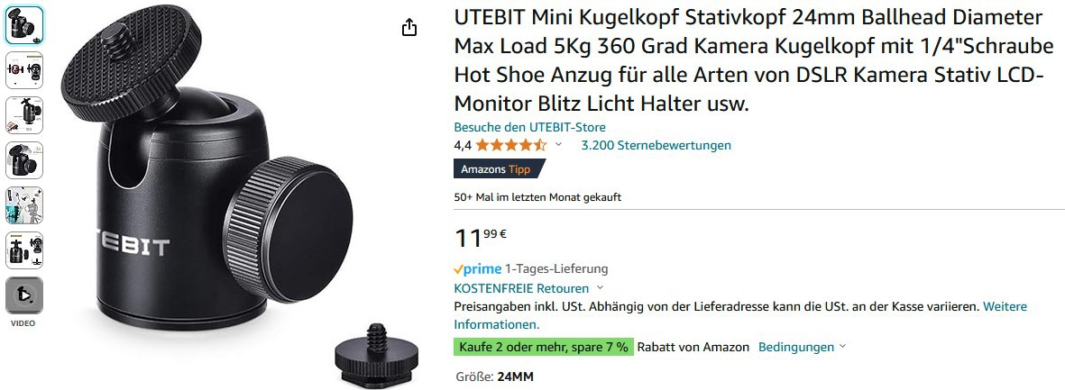
So I needed to design a better build plate to get a precise alignment. I ordered one of those ball-and-socket joints used in photography and designed a build plate mount around it. This worked quite well.

Next to the loose tracks and pads. At the beginning I tried to get a perfect layer of copper on the steel plate. It was a nice bright copper color and mirrored the surface of the steel plate underneath (all scratches on the steel plate appeared on the copper 1:1). But it seemed to be too smooth. So, having observed what happens when you turn the current up too high, which is that the copper becomes dark and dull and grainy, and initially thinking that this was a bad finish, I deliberately tried to achieve this finish.
As you hopefully can see in the picture, the dark copper parts are rougher than the brighter parts.

First I used a low current for a longer time to get a nice top surface where you solder later on. Then I increased the current to speed things up. The surface became duller, but still had a bright copper color. I then turned off the output of my power supply, set the Voltage to 30 Volts, turned it on for about 1 second, turned it off, waited a bit, turned it on for a second and so on. The color changed to a darker copper tone. I also put it under the microscope at various stages and the surface changed from basically the surface of the steel plate just in copper to a grainy dull surface. If I understand correctly, these grains are called nodules.
Now, this surface was rough, but sometimes when you ran your finger over it, you had some copper powder on it. The nodules seemed to be loosely attached to the copper. So after the 30 Volt treatment I went back down to slow mode to 'fix' the nodules.
As it is now over a year since I did this, I don't remember anything clearly. For example, I also reversed the polarity for a short time (which removed a little copper from the plate) and increased the voltage again, which I think seemed to roughen the surface even more. Perhaps the gas bubbles that form on the copper surface at such high Voltages cause the surface to become rough.
Another thing that I think helped was heating the resin. I think because it is more liquid it can creep under the grains.
End
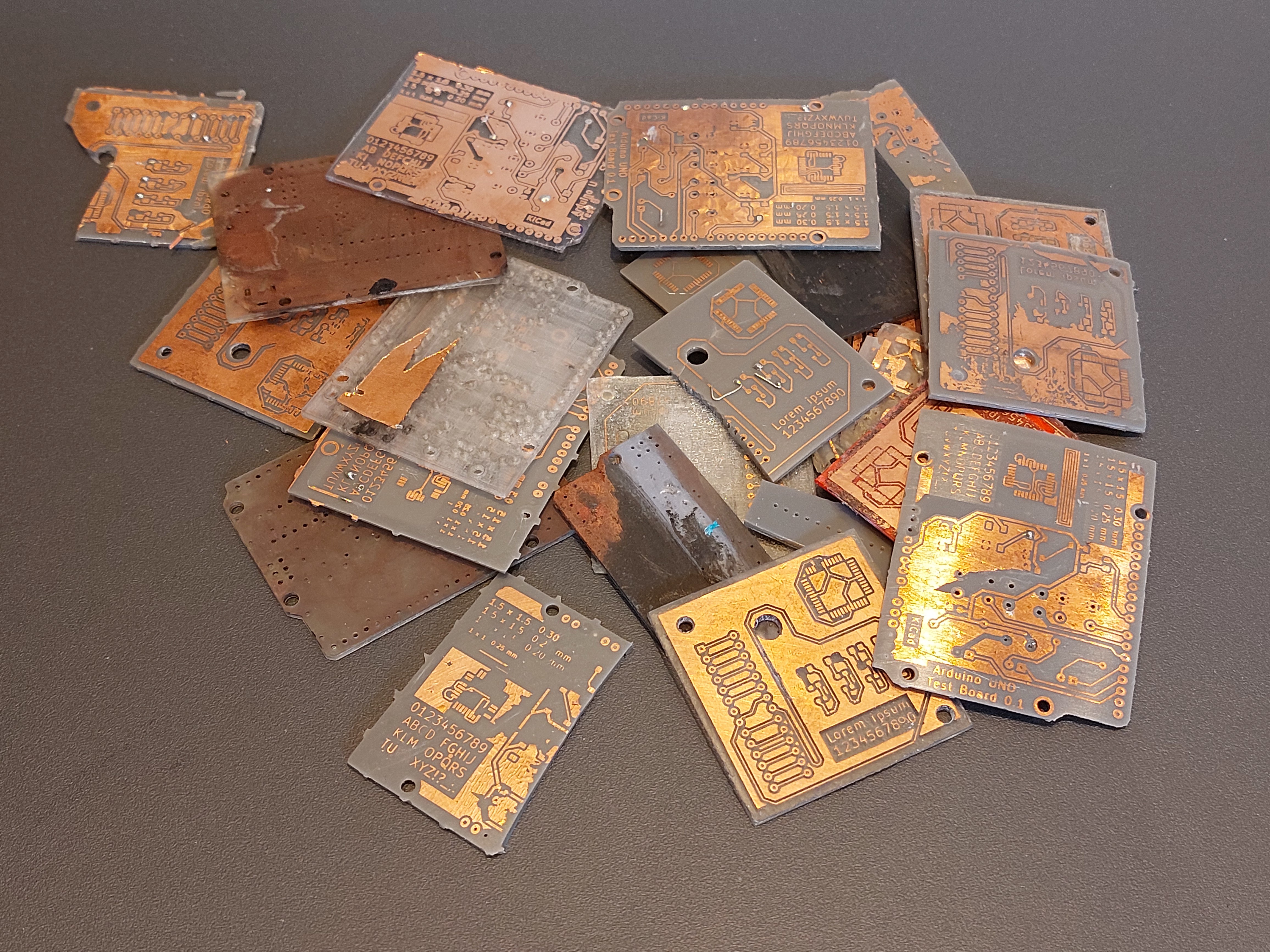
That is basically all I remember about what I did to get to the PCB in the pictures. I think it took ca. an hour to get the PCB in the picture.
The holes covered by the layout resin can be easily opened by sticking a needle or something into them.
A few weeks after I hadn't finished this project, I decided to try the glue method again. I had JB Weld now for another project and had read that it was suitable for high temperatures.
So I just printed the board with the holes, but with the holes closed on the first layer so the JB Weld wouldn't seep into them. Then I tried to apply a thin layer of JB Weld and pressed a sheet of copper foil over it. I didn't etch it and just tried to pull on the copper. To my surprise it was damn strong. The copper cracked instead of peeling off. I also applied heat with a soldering iron. It didn't weaken it, as far as I could tell. I was pretty pissed. All those weeks of experimenting (and money) because I thought it wasn't possible to glue copper to the board were basically for nothing.
A problem I could see with this though is that the holes are covered with a thin layer of JB Weld. I dont know if poking a needle into them could damage the copper around the holes.
Here is a PCB in action (ignore the bad soldering please, should have used more flux. Also it was a stupid idea to use those buttons on the wrong side, but it was a test layout anyway):
This is a small percentage of my attempts, the rest ended up in the trash. I also printed the board with clear resin (not high temp compatible) and it honestly looks super cool to have a clear PCB.

Another note
I was not working very scientifically here. So when I say that something didn't work, for example printing directly onto copper, it may well be that it does perfectly work, but my experiments were flawed. Maybe it's just that this type of resin doesn't stick well, or I just needed to heat it up, or even though I tried to get the oxidation layer off the copper as best I could, I didn't do it thoroughly enough.
So if you want to try it yourself, don't rely on anything I've said.
Other things I wanted to try but didn't have the motivation:
Double sided PCB, by printing the PCB half the thickness and then glueing two single sided PCBs together.
I let DeepL improve this text, because my writing is terrible. English isn't my first language either. What it obviously couldn't improve was my way of explaining things. Sorry about that.
Therapeutic whining (this has nothing to to with the project itself, just ignore this)
When I held the working PCB in my hand, my motivation dropped to zero. It's almost as if I now despised this project. The doubts about whether it was a novelty or useful at all were already there, but I still wanted to hold a working PCB in my hands, even if someone else had done it before, or if it was far too complicated and unreliable to be an alternative to traditional PCB etching at home or ordering it from a manufacturer.
I always struggle to finish things. When I have an idea, I hyperfocus on realising that idea. And as soon as I have an (ugly, unfinished, but working) version of that idea, I completely lose interest in it and somehow despise working on it. And also the doubts. Is it even a good idea, is it a novel idea, or is it already widely known and I am just reinventing the wheel? Is it even useful?
When I had the idea for the FDM toner transfer technique for example, I doubted its usefulness and novelty so much that I didn't put it online for months after I had successfully printed a few things using it. Besides, it's not that big a leap from PCB toner transfer to FDM toner transfer. I was afraid of comments like: "WOW, you've applied a known technique to something else, big deal, I bet you're proud of yourself, loser" (I still got a few comments like that, but after seeing that other people found it useful, my doubts diminished). I finally posted it on thingiverse a few months later, only because my depression was getting worse. Sounds weird, but my attitude was "yeah, if they hate it, I don't care, and if they like it, maybe I'll feel a little better". After I posted it on thingiverse, I think I got about 20 likes and maybe two comments. So I thought maybe it wasn't shit, but it didn't seem to be anything of interest.
Then, another year and a half later, I had another depressive episode and posted it on reddit. Well, on reddit I got a couple of awards and a couple of thousand upvotes, so all my fears and doubts were basically for nothing.
I feel the same way about this project now. I abandoned this project a year ago. I only took a few pictures and threw most of my attempts in the trash. I basically have no documentation. I forgot how to use the Python scripts I wrote.
When I have projects like this, I do a quick Google search to see if it's a common thing. If I can't find anything, I start the project and avoid to look up anything close to it. So far, I'm not brave enough to google "SLA printed circuit board" or anything like that, for fear of finding out that all the work and money I've spent is basically for nothing because someone else did it earlier and better. When I saw the post on reddit a few days ago by the guy who had successfully made the FDM printed circuit board with the wires, I felt physically sick, because I also tried it but didn't post it. So. For fear of someone else posting something like this in the future and making me physically sick, I'm posting this now.
If this is new and useful, and there are people who want to know more about it, my motivation to revisit this project will probably come back. But my fears and doubts now prevent me from putting any more work into it.
I currently have at least 10 projects that are working but aren't 100% finished. For some of them, all I need to do is take some nice pictures and put them online, but even that feels almost impossible for me, because I would have to tidy my room, find a nice background, and my phone's camera isn't that good and I haven't got good lighting, so it would probably look shitty, etc. Also I'm kind of a perfectionist, but am not good enough to satisfy this perfectionism. Like I won't be able to take those beautiful pictures and videos all those youtubers can, so why bother?
As I said, if I have too long a break in a project, like waiting for my custom PCB to come in from China, there's a good chance I won't finish it. So what I wanted to achieve with this was to be able to produce a simple PCB relatively quickly (while maybe ordering it from a manufacturer at the same time, but that would most likely be a double sided board then), so that I never have a break in the flow of the project. If I didn't hate cutting and drilling PCBs so much, and if it was just a rectangular board, it would definitely be an easier and faster way to just use photo resist coated PCBs. So all in all, I don't think it's that useful, but it's another thing you can actually do with 3D printing.
So this is less of a project description and more of a blog post of what I did a year ago. But again, if there's a demand for more info, like which resin, the electroplating recipe, etc., I'm happy to share what I remember.