 Scott
ScottWhile thinking about the features I wanted for my AVR Data Recorder, since it will be AVR based, I wanted to use as many feature of the on-chip peripherals as possible, so I came up with a preliminary list;
- 2 analog channels with programmable gain and attenuation
- bipolar inputs
- true RMS reading for complex A/C waveforms
- a means to accurately measure current through a device
- an analog comparator to detect “events” to start and/or stop data capture
- a high-current digital output for switching loads, perhaps driven by a low-frequency source
- a means to record data and “time stamps” to EEPROM
- a means to replay or dump the captured data
- a means to “set and forget” with a single push-button to start the data capture
- run on a rechargeable power source
- programability
- nice plastic enclosure with a front and back panel
- above all, use components that I already have in stock
To that avail, here are the parts I selected to accomplish those hardware requirements:
Enclosure: I happened to run across some nice “used” plastic enclosures at the local surplus electronics store. Some of them had existing PCB’s in them, which meant that there was internal mounting posts for those PCB’s. Since this was intended to be a “one off” project, I settled on a nice plastic enclosure measuring 5 x 5 inches with a removable aluminum front and back panel. I could make use of the front panel but the back panel was not going to suit my purposes. I did however, have some soft plastic sheeting that I could easily and accurately cut with a utility knife. With an enclosure decided upon, I removed it’s PCB and took some dimensional measurements to determine how much PCB area I would have available for components and off-board connectors.
 AVR Data Recorder

The enclosure is shown in the left photo above. I am getting a little ahead of my build here but the middle and right photos show the final front and back panels.
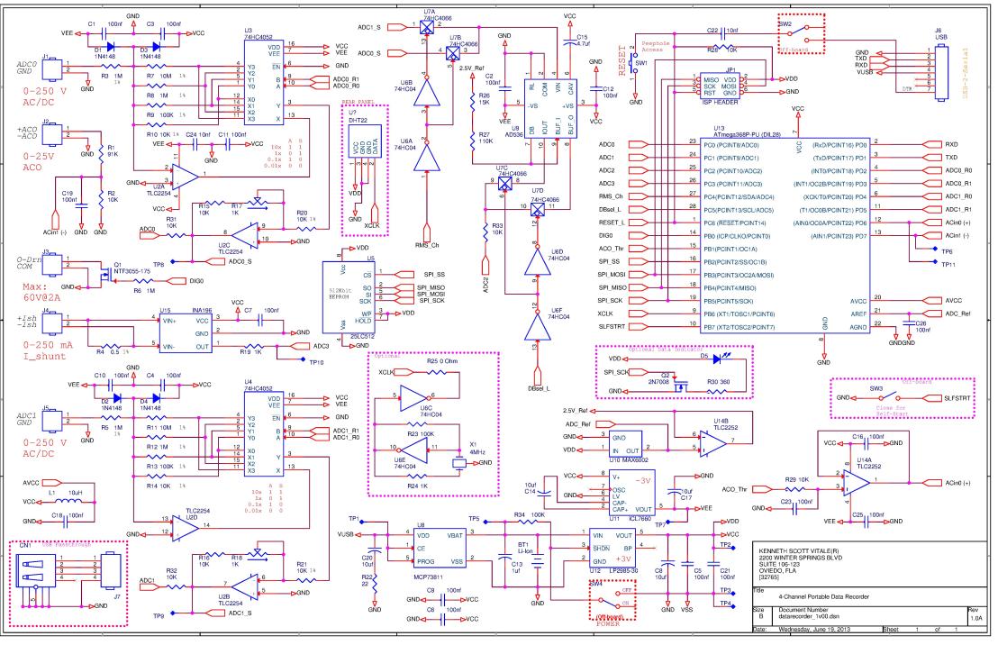 AVR Data Recorder Schematic V1.00A
The above schematic is available as a PDF file here.
2 analog channels: The ATmega328P (U13) contains a 10-bit ADC and can sample 9 channels plus “ground” (0.0 volts), the internal 1.10 volt reference and the on-chip temperature sensor. I would only be using 2 of the analog channels for the variable-range analog inputs because adding more would mean adding more gain and attenuation circuitry. Note that although the two analog inputs are “bipolar”, the ATmega328P is not. Meaning that the ATmega328P can only measure voltages between o.0 and “Vref” volts. In hindsight, I would have been better to select the ATmega32U4 because it does support “bipolar inputs” and has a built-in USB hardware interface.
Programmable gain and attenuation: The AVR’s input range is limited to it’s (internal or external) Vref, which means it’s input range would be only 1.10 volts. To gain a broader range, I elected use a 2.50 volt reference to extend the range between 0 to 2.50 volts. 2.50 volts maximum on the input is just not enough, so I would need an input attenuation circuit to measure higher voltages and an input gain circuit to accurately measure voltages that could be under 0.5 volts.
I already knew how to use operational amplifiers to create gain and attenuation circuits but what I needed was a way to program the gain. Decades ago, I had designed an ADA compliant PUBLIC telephone handset for the “hearing impaired”. In that circuit, I used a series of two MOSFET’s to switch different gain setting resistors (R7, R8, R9 and R10). I did not wish to use any discrete MOSFET’s if I could, so I decided to look into the 4000 series of CMOS logic. From what I recalled, there was the CD4066 and CD4052 analog switches, which I had used on other analog circuit designs years ago. I settled on the 74HC4052 (U3), which is a “Dual 4-channel Analog Multiplexer/Demultiplexer“. The typical “on resistance” at ±5 volts is 80Ω. In my calculations, the lowest resistor value in my gain circuit was 100 KΩ and had a 1% tolerance. 80Ω works out to be a 0.08% increase in the gain setting resistor, so at a 1% resistor tolerance, I did not see any need to be concerned as I was not designing a highly accurate piece of commercial or industrial equipment. Besides that, my measurements are limited to 8 bits with ±1 bits of conversion accuracy, which equates to less than 0.5% error, not including non-linearity errors.
The TEXAS INSTRUMENTS TLC2254A (U2A and U2C) used in the gain/attenuator circuit is an “Advanced LinCMOS RAIL-TO-RAIL VERY LOW-POWER QUAD OPERATIONAL AMPLIFIER” designed to be used as an analog front-end to Analog-to-Digital converters. The partial schematic below shows the gain and attenuation circuitry of one analog input channel.
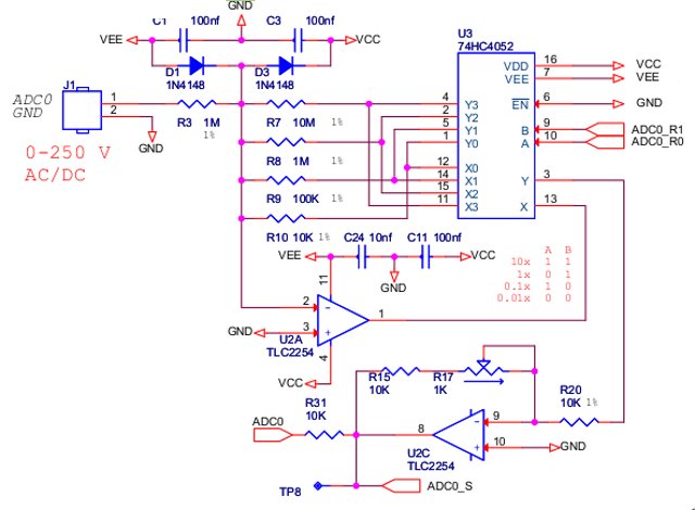 Excerpt – 1 of 2 analog channels
True RMS to DC conversion: I also had a handful of ANALOG DEVICES AD536A “True RMS to DC converters”. I thought it would be nice to add it so I could also measure complex waveforms, either true AC or AC on a DC bias. It will also work with a DC input, so that would get me the absolute value of the analog input. I decided to implement a means to measure the True-RMS on a separate ADC channel but allow a means to switch it between either of the two analog inputs. The AD536A has both DC and dBV outputs. Although theAVR Data Recorder can switch between either one, the dBV output needs amplification in order to be useful but I neglected to add a 2x amplifier on the output BUT the AVR can be switched to use it’s internal 1.1 volt reference instead of the external 2.50 volt reference but the accuracy has a ±10% accuracy. The internal reference’s long-term stability is not specified. The partial schematic below shows the AD536A (U9) using 74HC4066 (U7A/B/C/D) analog switches to select between the two analog channels (ADC0_S andADC1_S).
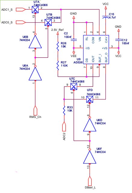 Excerpt – AD536A True RMS to DC
Current measurement: I happened to also have some TEXAS INSTRUMENTS INA196 “Current Shunt Monitor” IC’s left-over from a previous project. I thought it would be great to have a means to measure current, which could be read on a separate AVR ADC channel. I did not wish to have too large a shunt resistor because it would increase the shunt voltage. I also did not have enough room on the PCB to add extra circuitry to switch in various shunt resistor values and since most of the circuitry I was using had operating currents under 200 ma, I decided to use a 0.5 Ω / 5 Watt shunt resistor, which would give me a measurement range up to 250 ma. The partial schematic below shows the implementation of the INA196 (U15) and the shunt resistor (R4).
 Excerpt – INA196 Current Shunt
Analog comparator: The AVR has a built-in analog comparator. I thought this feature would be useful for detecting certain events and using them as a “trigger or halt the capture” mechanism. The input range would be limited to the supply rails of the AVR, which was 3 volts, so I thought it would be best to add a 10:1 voltage divider, yielding a 0 to 25 volt input range.
For the reference input, the AVR allows the selection of either an ADC channel or an external reference. I chose to allow access to both analog channels and create an adjustable reference voltage using one of the AVR’s PWM outputs filtered through a simple R/C network to derive a simple D/A converter. This way, I could set the reference input anywhere between 0 and 2.50 volts or translated by the 10:1 divider on the input, 0 to 25 volts. The partial schematic below shows the analog comparator input divider (R1/R2) on the left and the PWM R/C filter (R29/C23) and TLC2252 buffer (U14A) that creates the analog comparator’s reference voltage on the right.
 Excerpt – Analog Comparator and Reference
 Excerpt – ADC Voltage Reference
“External” ADC Voltage Reference: The ATmega328P has an internal 1.1 volt reference that can be used as the ADC reference. I wanted to have a full-scale reading of 2.50 volts, so I decided to use an external reference for that purpose. I chose to use a MAX6002 “Low-Cost, Low-Power, Low-Dropout, SOT23-3 Voltage Reference” as I have been using them on another project. The MAX6002 has a 1% accuracy and a long-term stavility of 50 ppm (over 1000 hours). The analog comparator’s PWM reference generator was using 1/2 of the TL2252, so I used the other 1/2 as a voltage follower to supply a voltage reference to the AD536A. The partial schematic on the right shows the implementation of the analog voltage reference using the MAX6002 (U10) and 1/2 TLC2252 (U14B).
 Excerpt – High-current Digital Output Driver
High-current digital output: In thinking about any extra features that I could stuff in to this project, and using every available I/O port and feature of the AVR I could come up with, I decided to add a means to switch a medium current load. I had a few higher-current MOSFET’s available in my sample stock but I wanted one that had a low Rds(on) and could handle at least 40 volts @ 1 amp. I found the NTF3055-175 (Q1) fit that role pretty well and so it was designed in. The NTF3055-175 has a 60 volt Vdss, a continuous Id of 2.0 A (@25°C), a maximum of 175 mΩRds(on) and maximum Vgs(th) of 2.0 volts, which works well for this application. It is configured as an open-drain output with the source connected to GND. Although technically, I should have used an opto-isolator to drive the MOSFET, I have not had any problems switching loads at 12 volts DC.
Because AttoBASIC supports both port level switching and DDS (direct digital synthesis) on the same I/O pin, I thought that the output could be used to either switch a load at frequencies between 1 Hz to 20 KHz or be switch on/off under program control, perhaps upon the detection of an event by the analog comparator. The partial schematic on the right shows the digital output circuit.
 Excerpt – EEPROM
Data capture storage: I had recently added a means to interface with an external EEPROM as a “data file” to AttoBASIC. One of the reasons was for use in recording data, such as the AVR Data Recorder. The “data file” is an external 64KB EEPROM that uses the AVR’s SPI (Serial Peripheral Interface) bus to communicate through. I used a MICROCHIP 25AA512 (U5) because I had a few in my sample stock. The partial schematic to the right shows the simple interface.
 Excertp – DHT-22
Digital temperature and humidity: After I designed, built and tested the AVR Data Recorder, I started to work with the DHT-22 (U?) temperature and humidity module. I added support for it into AttoBASIC and later decided to add it into the AVR Data Recorder, so this was an afterthought. The partial schematic to the left shows the simple 3-wire interface of Vcc, GND and the bidirectional “data” pin. Sadly, the DHT-22 is not DALLAS 1-Wire® compatible and has it’s own protocol, thus all the decoding “work” is done within AttoBASIC.
Support circuitry: The AVR Data Recorder was intended to run on a rechargeable Lithium-Ion battery source, specifically, the ICR18650NH type battery. These batteries carry a rating of 2200 mAh at a nominal voltage of 3.7 volts. I had salvaged quite a few of these batteries from DELL laptop battery packs that went bad. As is typical of laptop battery packs, usually only one or two cells actually go bad and the rest can be used. I decided that just one of these batteries would be sufficient for this project. I wanted to use a simple Li-Ion battery charger and MICROCHIP had a really simple one, the MCP73811 (U8) is packaged in a 5-pin SOT-23 housing and uses a single pin to set the charge current to either 85 mA or 450 mA. Since I would be using a USB interface to talk to the AVR Data Recorder, I could set the charging value to the higher 450 mA setting for charging from an external USB power supply or a computer’s USB interface.
Having only 3.7 volts (nominal) available from the battery, I chose to run everything off of 3 volts power supply. The LP2985-30 (U12) suited this purpose. The LP2985 series are “150-mA LOW-NOISE, LOW-DROPOUT REGULATOR WITH SHUTDOWN“. The suffix of “-30” means it is fixed to regulate at 3.0 volts. Although the LP2985 and MCP73811 run off the internal Li-Ion battery, I make use of the “shutdown” pin to power off the rest of the circuitry so the battery can be charged while plugged into a USB port or power-supply.
In designing the analog front-end for the two analog channels, I decided that it would be best to run all the analog components with a bipolar power supply of ±3 volts rather than a mid-rail reference running off of a uni-polar 3 volt power supply. Doing so would increase the accuracy and headroom of the analog front-end. The 74HC4052 (U3 and U4) needs a negative voltage when operating as an analog multiplexer, therefore it works well with the TL2254’s (U2) in the analog front-end. In order to obtain the bipolar power supply, I used the ICL7660 (a.k.a. MAX1040) “Switched-Capacitor Voltage Converters“. The ICL7660 is a REALLY old part and has been around for a very long time. If I am not mistaken, it was originally designed and sold by INTERSIL. The ICL7660 (U11) requires just two 10 uF capacitors, one as the “charge-pump capacitor” and the other as a”reservoir capacitor”. The schematic below shows the Li-Ion battery (BT1), MCP73811 (U8), LP2985-30 (U12) and ICL7660 (U11).
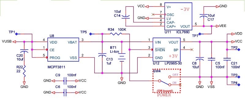 Excerpt – Power Supply
USB to Serial Interface: The AVR has an on-chip hardware UART with a TTL-level interface. My laptop does not have an RS-232 interface, most these days do not. I chose to hard-wire in a prefabricated CP2102-based USB-to-serial bridge module for that purpose. Doing so allows me to supply power to the AVR Data Recorder directly from the USB power pins.
In the next posting, I will discuss more progress on this project.
Peace and blessings.
Discussions
Become a Hackaday.io Member
Create an account to leave a comment. Already have an account? Log In.