 Ben Brown
For the user input, I am designing in a touch wheel similar to that of the older iPods.
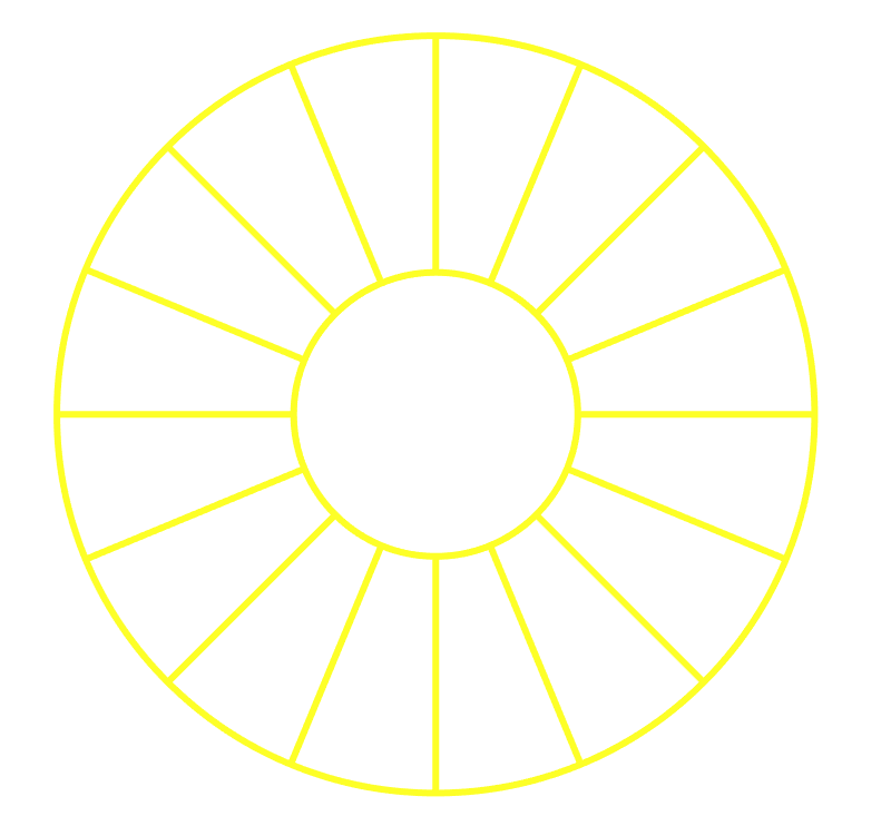
In the iPod the wheel is sensed by 16 sensing segments, and this number makes be happy being a power of two. Thus for this design 16 segments will also be used for sensing finger position, plus a center pad for the selection button (touch enabled as well).
To design our touch wheel, we want 16 evenly spaced segments around the wheel with a small distance between them. I used the polar grid feature in illustrator as I have access to it, however most graphics design software should be able to make a grid. I made the grid yellow, so that in the later stages it can be easily filtered out in the KiCad bitmap2component program. This is because we actually want where the grid is to become the spaces between the pads. I made the original circle 40mm wide in illustrator, however this can be scaled in the kicad software as well.
This is the picture that I exported (bitmap file so no compression).
I then opened this file in paint (or any other image editor would work), and filled in the white spaces where we want the copper to end up black. Black so that it is very easy to use in the kicad importer. This resulted in this file :

Next, importing this circle into the KiCad bitmap2component converter, make sure the DPI setting matches the exported image, and check the last tab shows what you expect to see. Except, note that because you are 'drawing silkscreen' you want the inverse (Tick the box), so that everywhere you see white on the image is where the copper will end up. The bitmap2component software does not let us directly export to the copper layer in our component, so i exported to the Eco1 layer and saved the file to my desktop.
Next open the file in a text editor of your choice and use find and replace to change all occurrences of "Eco1.User" with "F.Cu" and save the file.
This has now created a footprint with large copper pours, but with no pads we can connect to. To add connections to each copper section i opened the footprint in the editor and placed a pad in each copper section, remember to turn of the resist & paste layer on each pad to make sure you have a nice continuous solder resist over your pads.
Then I quickly made up a symbol for the part in KiCad and wired it up to the PSoC..
Discussions
Become a Hackaday.io Member
Create an account to leave a comment. Already have an account? Log In.