 Capt. Flatus O'Flaherty ☠
Here are some boards for putting together a basic 4G femtocell.
It would be very tempting to try and design and build a PCB with all the desired features from the very beginning and, in an apparent contradiction, there is actually a final design in progress as well. So what I have done is to split the project up into building blocks, mostly on separate PCBs or using PCBs with different blocks on different sides of the board. Confusing? - Yes, I am very possibly confused about what I am doing as it seems that I am trying to do the initial and the final stages simultaneously! There is however some logic to this, as l will try and explain.
Here below are the building blocks for stage 1 (There are already some more consolidated building block PCBs for stage 2, but I'm trying to ignore them at the moment ):
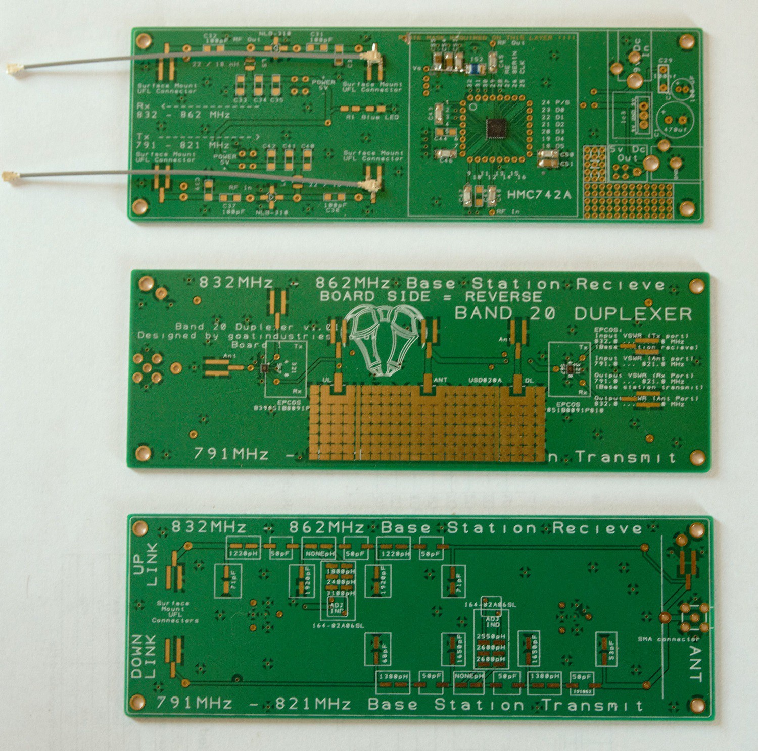 The top board has a couple of RF amp circuits and a power supply. The left hand RF circuit has a basic amp with no gain control which can be used in series with the other amp or on it's own. The big difference is that it's easy to solder. The middle circuit is another amp but it has digital variable gain control. I had the chip soldered in by a specialist company so that at the very least I had one possible error eradicated. I will try and solder subsequent boards myself and will use this board as a testing reference to compare and check my own soldering with a multimeter or oscilloscope. The two amp circuits were taken directly from the datasheets for the main component so all the passives (capacitors, inductors and resisters) were given by those sheets.
The middle board has an enormous band pass filter (BPF) pad on it which is factory tuned for high accuracy. It also has a couple of tiny 'cell phone' BPFs professionally soldered on, just to test the difference between the two options, one being big and expensive and the second being ridiculously small and 1/4 of the price.
The bottom board, which is actually the reverse of the middle board, has pads for home made filter circuits with one tunable inductor. This circuit is here just to prove to myself that we can't design and build our own BPFs because of the poor tolerances of the available components (mostly +-5%). It might even work!
The next log will look at another board that is already sitting on my table ready to be soldered up and that has some of the above features combined. Maybe stage 2 will work straight off, but if it doesn't, then I've got stage one as a good fallback. I give stage 1 about 70% chance of success and stage 2 about 50% chance.
One of the problems with working with PCBs like this is that the turn around time for manufacture is 10 days, including postage from China. For this reason it's good to try and be 10 days ahead of myself. Another problem is that some of the components are very hard to get hold of. The large BPFs are made in China for a USA company who only sell through one UK company so the supply chain takes about 3 weeks to navigate.
Discussions
Become a Hackaday.io Member
Create an account to leave a comment. Already have an account? Log In.