 Simon Merrett
SAFETY
A theme of Yapolamp is safety. I've already discussed the blue light risk that I'm avoiding and in this log I'm going to focus on making sure that my children don't find voltage and current sources where we don't want them.
THE ISSUE
Having thought about where various system components would be best placed I think the charging circuit should largely be off-lamp and in a charging/docking station. This is partly to minimise the components that would need enclosing on the main torch. I need some way of getting the battery charging power across to the Yapolamp. If I just leave bare terminals across the positive and negative 18650, however well recessed, Murphy's law says that my son will find a way to get his tongue to make contact with them. I will use a protected 18650 but the over-current protection is unlikely to kick in before I'd want it to. So the first part of the challenge is to find a way to charge the 18650 without disturbing the control mechanism of the Constant Current - Constant Voltage (CC-CV) charging strategy that also prevents back-feed from the battery to the charging connector.
The second part relates to the other side - the charger. The TP4056 is a CC-CV charger which the datasheet claims does short circuit protection across the battery terminals. Although this sounds like a decent default, I'd like to see if I can improve upon this.
OPTIONS
The most obvious option to me was a diode on the torch side. But this creates a voltage drop of about 0.7V for silicon diodes and 0.3V for Schottky diodes. If I understand correctly, this would lead to the Constant Current phase being prematurely ended (as the battery won't actually see the 4.2V detected at the charger) and the CV phase will end with the battery at a far too low voltage for a full charge (e.g. 3.5 - 3.9V).
So then I looked for an option which didn't create a fixed voltage drop. A MOSFET is appealing because the voltage drop across it is proportional to the current across it and can be very low, especially for the low current likely to be seen at the end of the Constant Voltage phase. I wasn't sure a low-side MOSFET switch was a good idea from the perspective of keeping a common ground in the charging circuit (that's me being wary, I don't know if it would cause an issue in reality). A high-side P channel MOSFET switch sounded like a good idea until I found out that using a reversed MOSFET for reverse polarity protection won't help in a back-feed protection scenario as the thing conducts in both directions. What does apparently work to prevent back-feed is an "ideal diode". I found a schematic for an ideal diode circuit and although an IC is used, it is shown as a pair of PNP transistors: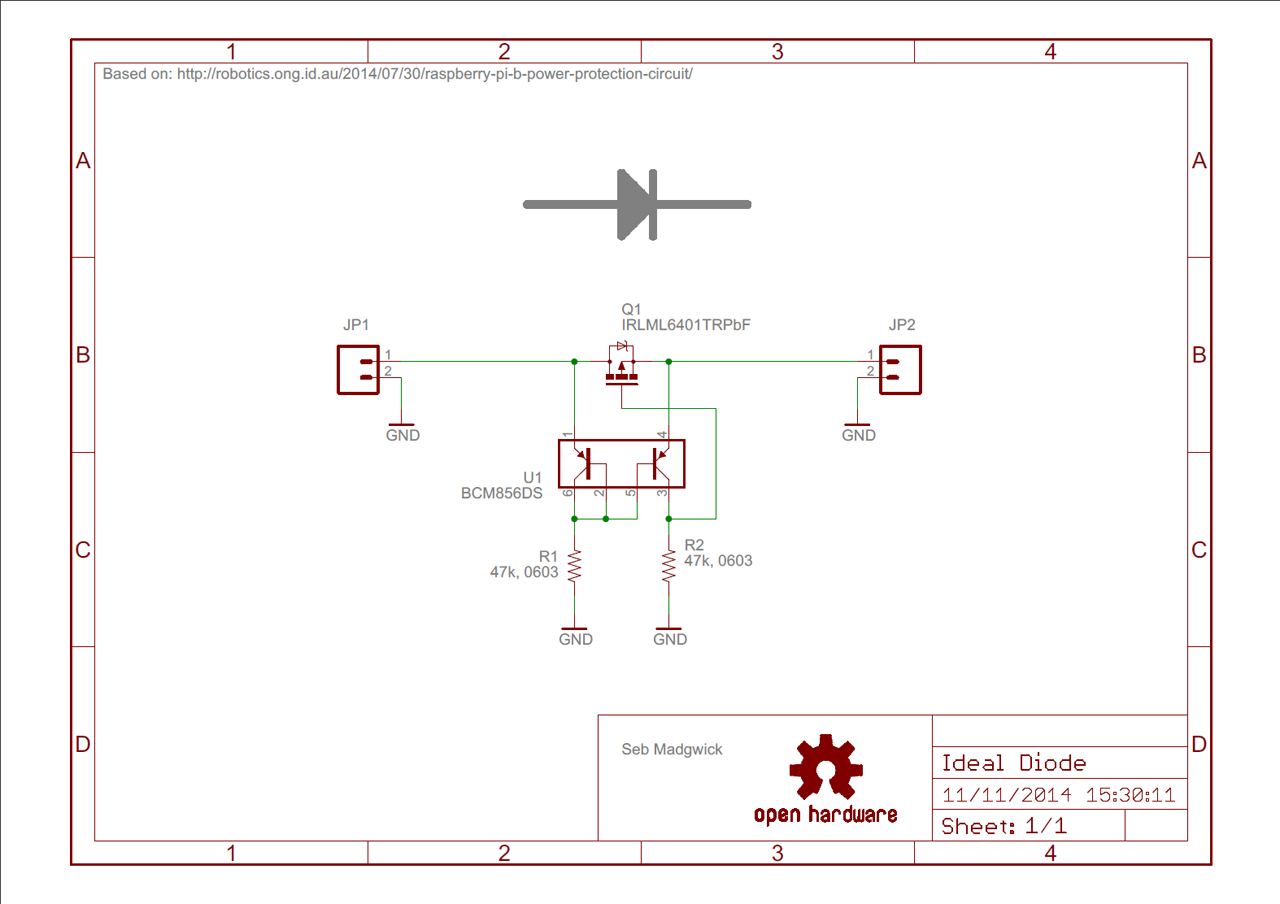 By Courtesy xioTechnologies at Github https://github.com/xioTechnologies/Ideal-Diode, Fair Use
The ideal diode is a nice idea but it doesn't help us with the charger side of the circuit. Thinking about high side MOSFETs and a way to ensure that both the torch and charger were required before either would allow voltage/current to reach the connections, I came up with the idea of a high side N channel MOSFET on both the battery side and the charger side. On the charger side, it would be in the normal switching direction, with the Drain towards the TP4056 +BAT and Source towards the battery terminals. For the battery side MOSFET, I (think I) would have the Drain towards the battery positive terminal and the Source towards the TP4056 MOSFET. Both MOSFETs would have their Gate's pulled low to Ground by suitable value resistors (10k?). It might look like: The reversal of the MOSFET on the battery side should still allow current to flow into the battery if it is driven into linear mode. This brings me onto driving the MOSFET. For a high-side N channel MOSFET, I need to lift the Gate voltage at least to Vds + VgsThreshold. For my prototyping n channel MOSFET (IRLB8743PBF) is > 4.2 + 1.8 = 6V and in reality we want about 7V to be sure (the datasheet Ids vs Vds graph doesn't really cover our ~1A charging current; the graph starts at 10A).
BOOST!
At the moment, my highest voltage comes from the 5V USB going into my TP4056 module. With my new-found bravery in the world of analogue circuits, I looked around for a charge pump to drive my N channel MOSFET gates. You can get bespoke ICs for managing this but you can also make charge pumps in the form of voltage multipliers. These voltage multipliers often require an AC input, with an inverted part of the signal. I don't want the complication of this but I did find one design that could work nicely with a simple square wave and act as a nominal voltage doubler. The design is called a Dickson voltage doubler and apart from diode losses (you could make one with MOSFETs instead of diodes for less of a voltage drop), this circuit should take you to double your input voltage for low currents (which is perfect for our application of driving a MOSFET Gate):

By Courtesy Spinningspark">http://en.wikipedia.org/wiki/User:Spinningspark">Spinningspark at Wikipedia, CC BY-SA 3.0, Link
The Clock line is where you feed your voltage in. Here's one I made in LT Spice: I have assumed that the Gate current is 0A because we aren't doing fast switching here. This is what the 500Hz clock signal appears to give us in increased voltage across C2:
 7.7V seems very usable to drive our high-side N channel MOSFETs. And this is where I think this could be a nice system - we need the square wave to come from somewhere. Although some designs for charge pumps and voltage multipliers use a 555 timer, I already have the potential to produce a square wave from my microcontroller on-board the torch. The potential beauty of this system is that the Gate drive voltage can only be delivered (and allow voltage/current at the connections) if both the square wave from the microcontroller and the voltage doubler circuit are correctly brought together. We'll need another couple of connections over the physical interface for the drive voltage to reach the battery-side MOSFET and the square wave pulse from the microcontroller to reach the Dickson doubler capacitor C1.
So that's my plan for the next stage of exploration...
Discussions
Become a Hackaday.io Member
Create an account to leave a comment. Already have an account? Log In.