 agp.cooper
TD4 OpCodes
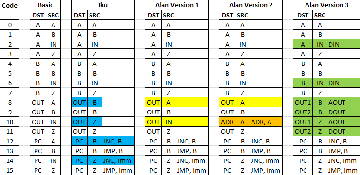
The TD4 opcodes are designed for minimum decoder chip count (2) and therefore only 12 of the 16 possible opcodes have been mapped (at least that is what the text suggests):
Immediate OpCode Mnemonic   ; Comment
DCBA      0011   MOV A, Imm ; MOVE Imm to A register
DCBA      0111   MOV B, Imm ; MOVE Imm to B register
0000      0001   MOV A, B   ; MOVE A register to B register
0000      0100   MOV B, A   ; MOVE B register to A register
DCBA      0000   ADD A, Imm ; ADD Imm to A register
DCBA      0101   ADD B, Imm ; ADD Imm to B register
0000      0010   IN A       ; Copy input port to A register
0000      0111   IN B       ; Copy input port to B register
DCBA      1011   OUT Imm    ; Copy Im to output register
DCBA      1001   OUT B      ; Copy B register to output port
DCBA      1111   JMP Imm    ; Jump to Imm
DCBA      1110   JNC Imm    ; Jump to Imm if C flag is not 1
I found however, author (Iku Watanabe) has actually mapped 14 of the 16 OpCodes!
You will note that the OpCodes always add the Immediate value to the source register so if an immediate value is not required then it must be set to zero.
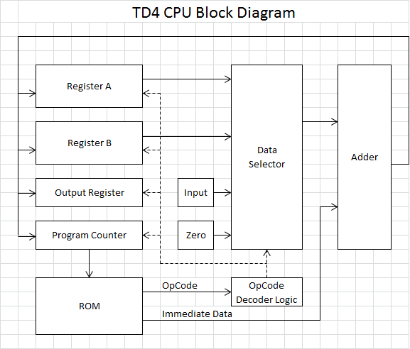
Here is a CPU block diagram of the CPU:
Remapping The OpCodes
Let us begin by using format [DST][SRC]. The results in the following mapping:
DST    SRC    Comment
A    A      Move A     + Immediate to A
A    B      Move B     + Immediate to A
A    IN     Move Input + Immediate to A
A    Z      Move Zero  + Immediate to A
B    A      Move A     + Immediate to B
B    B      Move B     + Immediate to B
B    IN     Move Input + Immediate to B
B    Z      Move Zero  + Immediate to B
OUT  A      Move A     + Immediate to Output
OUT  B      Move B     + Immediate to Output
OUT  IN     Move Input + Immediate to Output
OUT  Z      Move Zero  + Immediate to Output
PC   A      Move A     + Immediate to PC
PC   B      Move B     + Immediate to PC
PC   IN     Move Input + Immediate to PC
PC   Z      Move Zero  + Immediate to PC
You should be able to see that for some OpCodes, they only make sense if the Immediate data is zero.
OpCodes
I have mapped the set of basic OpCodes (as shown above), Iku's OpCodes and two of my own OpCode transformations:

(If you like, each step across the table adds one chip to the decoder design.)
My first transformation is to honour Iku's OpCodes but to release the unused OpCodes.
My final transformation is to add an address output register.
Now it is not absolutely necessary to take my approach as you can just use the A Register value to directly apply the RAM address, but for a CPU with so few registers an extra register is probably worth the extra two or three chips.
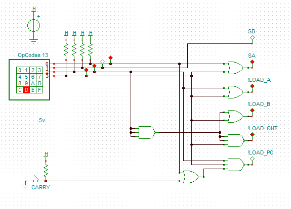
Here is the Iku decoder:
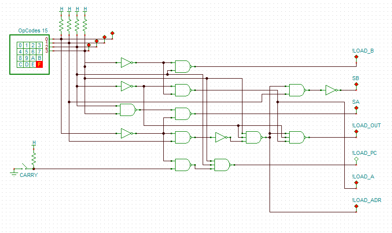
And here is mine (version 2):
Although mine has four chips instead of two, it does release a spare inverter and nand gate which I will need for the RAM databus decoding. That is, in order to access the RAM I need to have a tri-state databus, I will need to swap the Output 74LS161 with a 74LS173 and provide output logic to tri-state the output buffer when a memory input is preformed. Sounds hard but it is just an inverter or two.
The Clock
Iku has the PC clock in phase with the other clock signals, for most of my CPU designs I have it out of phase. It works because all outputs are shunted via the adder and delayed, making the clock/data transition reliable. As I have found out, this will also work for the !WE and !CS of RAM that does not have an !OE. It could be tricky in some cases if the buffer has a data hold period greater than the data delay. Something to watch out for.
Final Version
How many times have I said that?
Anyway, I worked out a simpler way. I can demultiplex the OUT signal using ROM_D4 (Version 3):
I have also renamed the label to suit access to a 16 bit RAM (74LS189). Yes that was 16 bit (not 16k or 16M). You could use a 74LS138 to do this but I used a 74LS02 (quad NOR gate) as I want to invert the select and create a !WE signals. Here is part of the schematic:
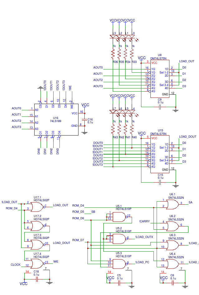
You should recognise Iku decoder to the bottom right and my demultiplexer to the bottom left. I have also swapped out the 74LS161s for 74LS75s as I need to invert the output for the 74LS189 RAM. As I am using LS TTL the inverting outputs of the 74LS75s work better with LEDs. I have added the CLOCK signal to the !WE to minimise propagation delays to the RAM. I used the 74LS75s as they are a transparent latch and I need the output from them ASAP (not the next clock cycle).
Chip Count
Iku's TD4 has 13 chips but I have 17:
- I gain one because I swapped 2x 74LS138s for 1x 74LS154.
- I swapped the 74LS540 for a 74LS14.
- I swapped two 74LS161 for two 74LS173 (Registers A and B).
- I swapped a 74LS161 for a 74LS75 (OUT1 or AOUT).
- I added a 74LS02 to decode the second output register (OUT2 or DOUT).
- I added another 74LS75 for the second output register (OUT2 or DOUT).
- I added a 16 bit RAM (74LS189).
So all in all I am very happy with the result.
AlanX
Discussions
Become a Hackaday.io Member
Create an account to leave a comment. Already have an account? Log In.