 Yann Guidon / YGDES
The experiments with the RES64 are on hold, waiting for the delivery of more/new parts (and the strikes in France make the delivery date even more uncertain) so I'm back to the ASIC side of the projet. There is significant progress with #VHDL library for gate-level verificationand some early results are "interesting" and require more analysis.
To ease this analysis, I'm forced to split the carry-lookahead adding tree from the ROP2/Pass logic, which I'm going to re-synthesise now. You might remember the log That ALU should be good (03/25/2019) and the following diagram :
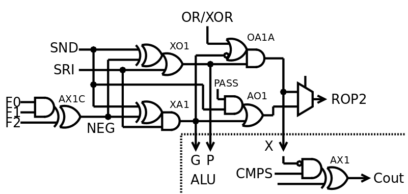
Well, it works nicely with the A3P family's gates/tiles but it doesn't fly as well with full-custom gates. I tried to get the gates complexity down to simple ones (like NAND2 and NAND3), even trying to eliminate the output MUX2, and did some bubble-pushing.
Remember that this logic unit has deep ties with the adder logic : P and G provide the Propagate and Generate inputs, and the X output is used at the output stage as well. The rest is built around these fundamental, shared functions. I know well it is possible to create a boolean unit with only 4 NAND3 (see http://www.6502.org/users/dieter/a5/a5_2.htm) but that circuit provides only one of these functions at a time, when I need 3.
Another choice for the ROP2 part is to enable the output only when required. This makes ORing more practical, we can combine more data sources later with lower constraints (the fan-in is higher and the combining gates are less complex).
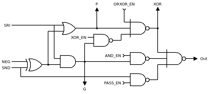
Starting from the output, I have made a big OR3 of AND2s, which were reduced to 2 layers of NANDs.
There are more control signals but this allows the output to be zero if nothing is enabled. More OR3s can be cascaded to inject data in the result bus.
I could push the bubbles further down the inputs but the P and G signals have a significant fanout so it makes more sense to simply put a buffer :
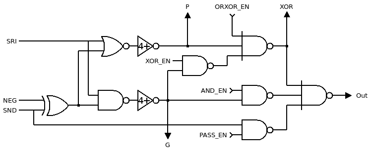
The other gates have a fanout of 1 (except the XOR2 at SND) so they can be simple, FO1 gates. The P and G gates can be OR and AND gates with FO4 or more, if needed, because they are a combination of a NAND2 and inverting buffer.
I have to redesign the control signals but that's not really a problem. There are more gates but they are "simpler". The new system is less adapted to ProASIC3 tiles but that's not the point. The new problem however is that when ADD/SUB is executed, the ROP2 output will contain the XOR value, which should be disabled somehow (if we want to use OR-combining only, not MUXes), unless another parallel NAND2 provides the value to the sink circuit...
The front-end XOR2 could be a XNOR2 if it's faster. In this case it's just a matter of adding an inverting buffer or something like that after the decoder...
OK, problem solved.
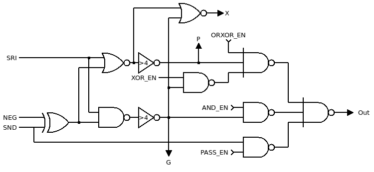
The XOR value is output unconditionally on the dedicated port, while the ROP2 output is cleanly enabled by ORXOR_EN, AND_EN and PASS_EN.
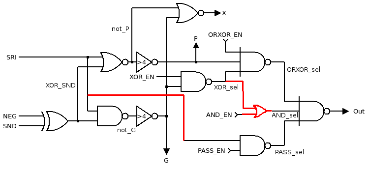
While implementing the unit, I found that there was some undesired redundancy :
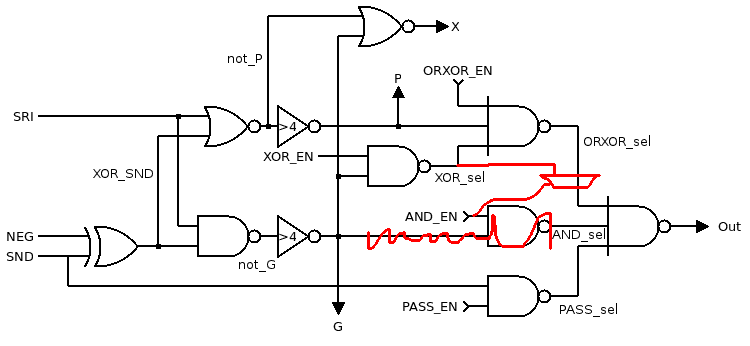
The goal is to 1) reduce the fanout of G 2) avoid having 2 identical gates with one shared output, while there is "room" a bit later in the circuit.
There would not be a MUX2, but probably a OR gate, which usually requires 2 levels of inverter but it's not in the critical datapth.
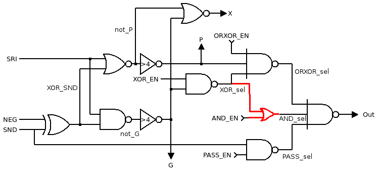
Decoding becomes a bit more complicated as well but... it will be easier for place&route :-)
Erratum : SRI is the bypassed signal, not SND !
How did this mistake manage to survive this long ?
The truth table is pretty nice
       NEG  PASS_en AND_en XOR_en OrXor_en
OR      0      0      0      0       1
XOR     0      0      1      1       1
AND     0      0      0      1       0
ANDN    1      0      0      1       0
SUB     1      0      1      x       0
ADD     0      0      1      x       0
PASS    x      1      1      x       0
clear   x      0      0      0       0
Notice that I changed the order of the boolean operations (again) to make decoding easier.
I'll have to redesign the equations and decoder very soon.
ROP2 is 11 gates per bit, or a massive 88 gates for the whole unit. Fortunately it is quite easy to layout...
Discussions
Become a Hackaday.io Member
Create an account to leave a comment. Already have an account? Log In.