 Keith
KeithThe second master we look at is the SC008, see Figure 6.27. This board uses the Motorola 68008 processor, IC16, which is the 8-bit version of the powerful 16-bit 68000. Although its data bus is only 1 byte wide, the 68008 uses the same mnemonics as the 68000 and so is software compatible. The chip has 22 address lines and so can access 4 Mb of memory space. Like the STEbus, the 68008 acts on the data acknowledge principle. When it accesses a location the processor waits for a /DTACK signal which terminates the cycle. While waiting for /DTACK the 68008 goes into a wait state; note that the processor clock continues to operate whilst in this state so that the 68008 will not lose the contents of its registers if a cycle takes a long time, in contrast to the 6809. The /DTACK line is open-collector, and three devices can drive it LO - the UART (IC18), the ROM or RAM from the PAL (IC22) and the STEbus control PAL (IC6). Alternatively a cycle can be terminated by /BERR (bus error), which is linked to the STEbus TRFERR* signal thus if an error occurs on the STEbus then the 68008 is informed of it.
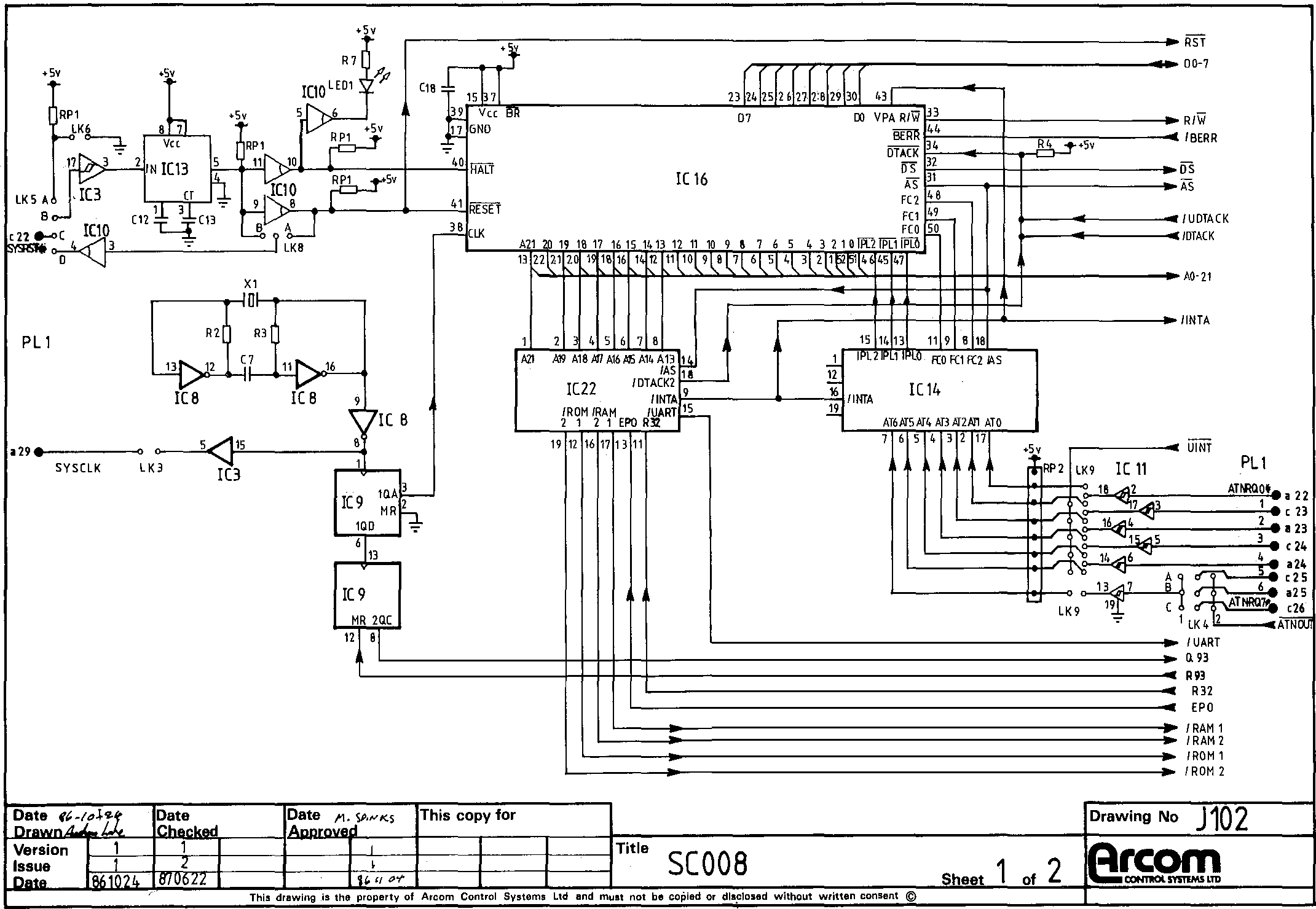
Figure 6.27a The SC008, a 68008 STEbus CPU board.
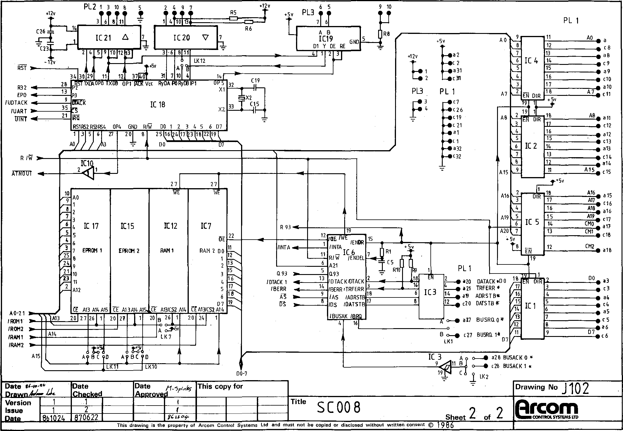
Figure 6.27b The SC008, sheet 2.
The other PAL on Figure 6.27(a) (IC14) is an interrupt encoder. The STEbus ATNRQ*s come onto the board via IC11 to link area 9, where they are joined by the interrupt line from the UART (/UINT). The ATNRQ*s and /UINT can be jumpered to drive the AT0-6 inputs on the interrupt encoder PAL. The PAL looks at AT0-6 and produces three outputs (IPL0-2) which encode the highest-priority interrupt, in a similar way to the PAL example in Chapter 4. In response to an interrupt the 68008 can generate an interrupt acknowledge cycle to retrieve a vector from the bus. Actually the SC008 does not have interrupt acknowledge capability. Instead, in response to an interrupt acknowledge cycle IC14 generates an /INTA signal which is fed into the VPA input of the 68008. This causes the 68008 to fetch an ‘auto-vector’ from a fixed point in its memory map. The CPU then vectors off to that location to commence the interrupt handler.
IC18 is the UART (68681), which derives its baud rate from a crystal (X2) and so can work at 9600 baud and beyond (unlike the 6850 on the SC09 which could only manage 4800). ICs 20 and 21 are the RS-232 driver and receiver chips. IC19 is an RS-485 chip; RS-485 is a transmission protocol like RS-232 but the transmitting device can be tri-stated so that the line can be shared by many transmitters.
IC8 (74S04) provides the 16 MHz STEbus SYSCLK, and is divided down by IC9 to give an 8 MHz processor clock. The second half of IC9 is a bus-timeout circuit. The MR (master reset) input is connected to the output enable pins of the STEbus driver chips. When an STEbus cycle is in progress MR will be LO so the second half of IC9 can count. After about 8 µs 2QC will go HI indicating that the STEbus cycle has taken too long, so something must be wrong (a bus-timeout has occurred): 2QC goes into the STEbus control PAL (IC6) which then asserts /BERR to terminate the cycle, rather than waiting interminably for DATACK*.
IC6 is the STEbus control PAL. When the processor asserts /AS and /DS and A21 is HI the access is deemed to be for STE. IC6 then drives /ENDR (enable driver) LO, which enables the STEbus drivers (ICs 1, 5, 2 and 4). After a delay given by R1*C5 /ENDEL goes LO and IC6 then asserts ADRSTB* followed by DATSTB*. When a DATACK* or TRFERR* is received IC6 releases the signals in the order DATSTB*, ADRSTB* and /ENDR. The SC008 does not have an STEbus arbiter, so cannot accept BUSRQ*s. When it wants to use the bus IC6 asserts /BRQ which can be linked to either BUSRQ0* or BUSRQ1*. LK2 selects which BUSAK* signal the SC008 should monitor, and by making LK2C the SC008 acts in a ‘permanent’ master mode and always assumes it has control of the bus. This mode can only be used when the SC008 is the sole bus master. Notice that CM1 is simply A20, so STEbus accesses with A20 LO will produce I/O accesses, and with A20 HI they will be memory accesses. Thus, as with the SC09, a processor without any specific I/O instructions can perform STEbus I/O accesses by defining an area of its memory map to produce I/O cycles.
Discussions
Become a Hackaday.io Member
Create an account to leave a comment. Already have an account? Log In.