 Rue Mohr
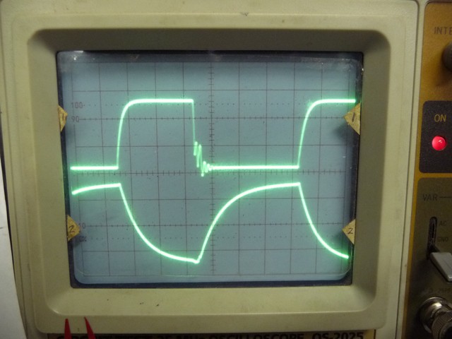
So, I been wrestling for quite a while with the pwm genorator trying to get rid of little glitches and bounces and ringing that came up during final assembly. The final straw was a 40mv, 5Mhz ring that caused the pwm comparitor to output a ring that the driver would pick up on. In the process I found out that as the control input votlage got close to 100%, the oscillator would change freq and slip thru another glitch that would double clock the flipflop causing th pwm to be split up wrong.
ARGKGH.
Has to be another way.
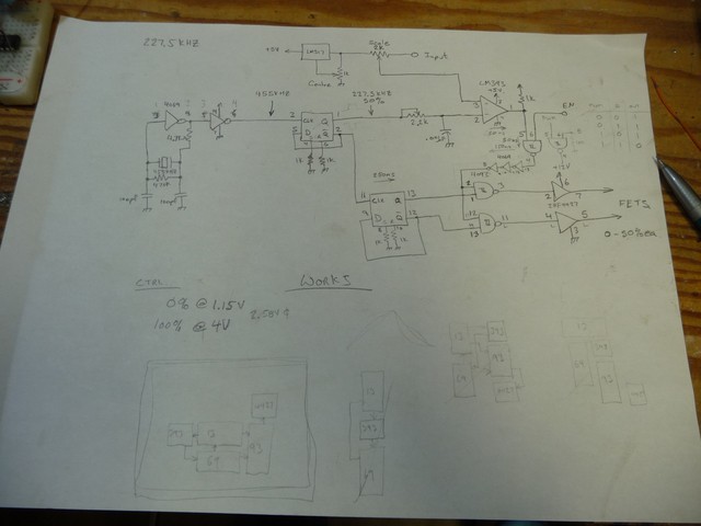
Sitting down and thinking, an idea occured. my origional design uses a ramping oscillator to also generate a square wave. What if I did this the other way around, took a nice reliable square wave genorator, and put it thru a RC filter to generate a ramp. its much easier to generate a stable stable square wave osc, I could use a 1 MHz crystal and divide it down to the 250Khz.
It also occurred to me that I had some low freq ceramic resonators, possibly one perfect for the job.
455Khz, is a common one, /2 = 227.5Khz, which is close enough to my 250Khz smps goal. quite a bit of the problems from the origional design were caused by the overshooting of the TTL logic gates, this is fine for a digital circuit, but this circuit is a hybrid.
CMOS to the rescue, its slower, its transitions are underdamped, and so its less noisy, no 5Mhz ringing.
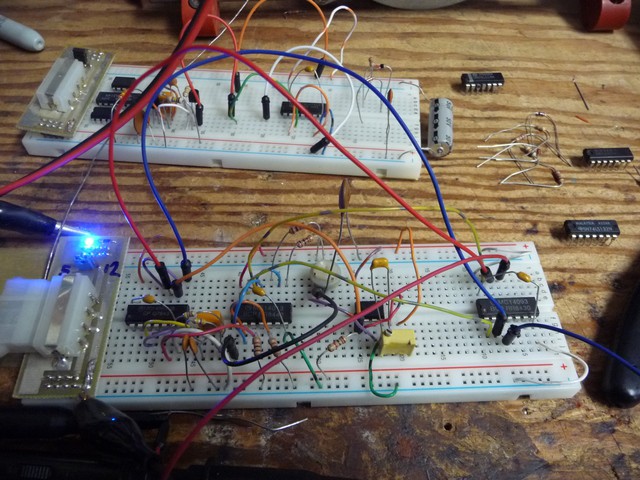
The basic theme is the same, there is a osc that outputs a square wave and a ramp, the ramp is fed into a pwm comparitor, the square wave divies up the pwm into two channels that go to a driver.
Its assembled and it works great. In the process I had two surprises.
1) The input of the LM393 draws a "LOT" of current when it crosses over its threashold, enough to throw out high impedence input signals, this is what was causing the osc in the origional circuit to freak out.
2) propigation delay. I actually had to add 3 inverters in the circuit to make up 150ns of delay and align signals, never had to do that with a circuit before.
It turns out this is a nice circuit, by adjusting the resistor on the RC, you can trim the amplitude of the pwm ramp. I put an offset and scale control on the main input to help match the two siganls.
New veroboard, start again,
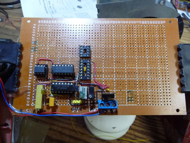
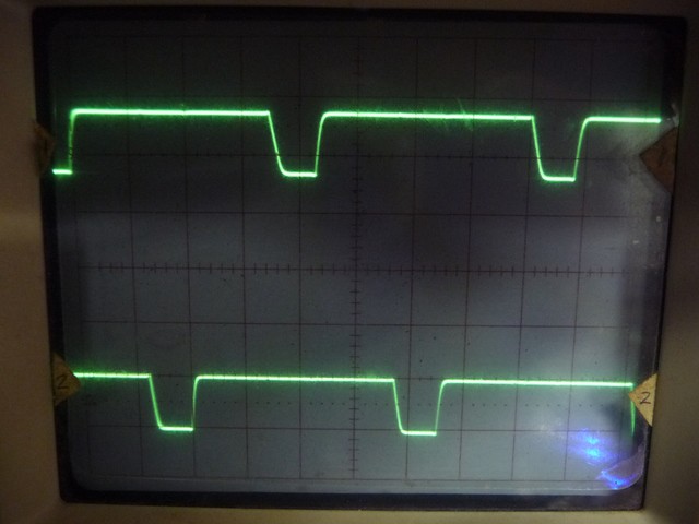
(old pic) its finished, the outputs look great. I get from 0-100% between the two channels with NO little glitches anywhere thru the duty sweep.
I'm just re-assembling my fet driver (post driver chip) to make sure its good with the driver chip and I can finish the power converter.
YAY!
But the question arises, could I have used two syncronized 3842 open loop to generate the pwm? [hint: its too late to ask this question]
Discussions
Become a Hackaday.io Member
Create an account to leave a comment. Already have an account? Log In.