 zaphod
a lot has happened since the last real project update, for starters I took this project to Maker Faire, photo:
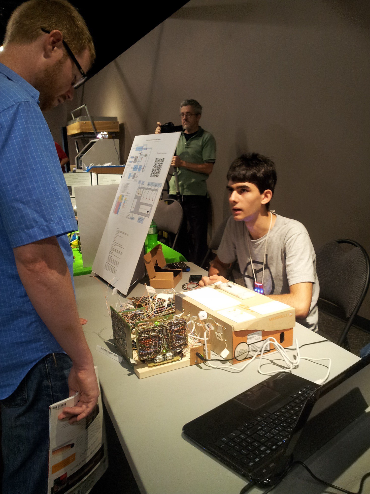
I had a great time at Maker Faire and got to have a lot of interesting conversations with a lot of interesting people.
now, on to the interesting stuff.
in my last project log that actually discussed the construction of the computer I mentioned that I was attempting to build ROM access logic in the form of a 1:16 demultiplexer, as you may recall I was attempting to use this design:
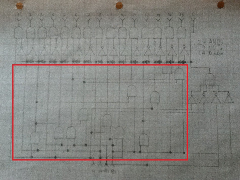
(the red box shows how much I built)
I didn't have enough prototyping space to test the entire multiplexer, but the preliminary tests seemed to indicate that it would work, so I went ahead and built what is shown in the red box above. once it was built I started to realize that it had some pretty serious problems, first off due to the low gate fan out of RTL I wasn't getting usable signals out, in addition it turns out that the chain of diodes quickly degraded all signals passing through, even when I used diodes with low forward resistance. eventually I decided to abandon this design and take a look at how real multiplexers are built. my research came up with this design:
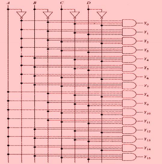
this design has much lower gate fan out and a much more predictable pattern. once again was unable to do a full scale test due to limited prototyping area, but the small scale results looked good so I went ahead and built it:
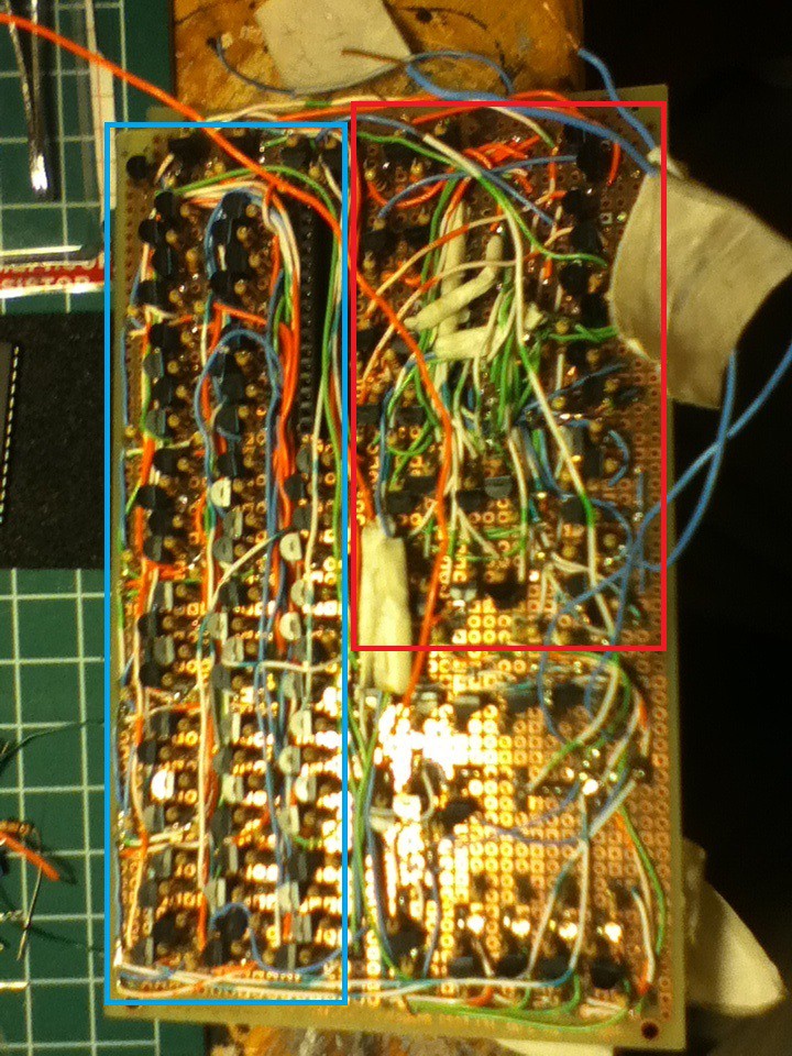
the red box show my (now abandoned) first attempt at the multiplexer, the second blue box shows the newer multiplexer design. the new multiplexer design seemed to work much better. the way that I tested the circuit was to connect the 16 outputs to 16 LEDs and then step through each address, this seemed to work and it appeared that only one LED light up at a time, just like in my small scale test. all good. I then proceeded to test the outputs with my first prototypes of ROM logic. this is where things started to fall apart. lines that had appeared to be off when attached to LEDs during testing where no seemingly on when connected too the next stage of logic. for a while I couldn't figure out what was going on, the LEDs seem to usally respond similarly to logic gates so I figured that the LEDs would be a good indication of what lines where on and which where off. I started probing around the circuit and found that some of the LEDs that were 'off' actually had enough voltage to be considered a logic 1 by the logic circuits I was connecting, but not enough voltage light up brightly. ideally I would have seen the dimly lit LEDs in my small scale testing, but as it turns out my desk lamp was bright enough that it overpowered the dimly light LEDs in both the small scale and large scale tests making it appear as though the circuit were functioning, when in fact it was not. because of this I didn't think to test the signals coming out of the multiplexer. the reason that I was getting a voltage in between my logic levels has to do with the construction of the four input AND gates used in the multiplexer. each AND gate consists of four transistors. the first has it's collector tied to VCC and the next has it's collector tied to the emitter of the first, and so on, until the emitter of the last transistor becomes the output, with the bases of the four transistors acting as inputs, the problem arises when the first three inputs are a one an the last one is a zero. the base-emitter currents of the bottom three transistors add up to produce a signal that is to high to be a zero and to low to be a one, hence the messy in between logic. at this point in the project I did not want to rebuild the multiplexer yet again and so I elected try and fix the problem with some analog engineering. eventually I managed to figure out that the part I was looking for was a comparator. this would allow me to set a threshold voltage and then repair all of my logic signals. I did attempt to build a comparator out of discrete components, but was unsuccessful so I ended up using integrated circuits, (blasphemy!) specifically the LM339 comparator. this did fix the problem and allowed me to move onto the next stage, ROM.
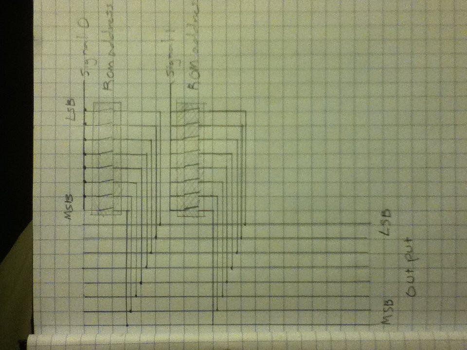
my idea for the ROM was to use 16 dip switches, each one playing the part of one ROM address. to implement this I thought I could build it like so:
I though I could bridge all off the pins on one side of the dip switch and connected them to the appropriate line on the multiplexer (address zero to line zero on the MUX, address one to line one on the MUX, etc.) from there I could set any number of the switches and when that line from the multiplexer went high I would only get a signal from the switches whose contacts were closed. I could then do this for all 16 addresses and connect the each line out of the banks of switches to the corresponding line on a larger bus, I.E. MSB of address one gets connected to the MSB of the bus forming a circuit that looks like this:
(once again unable to rotate photo)
with this design if signal line 0 was high and switch 2 (of address one) was closed line 2 one the output bus would go high. when the clock pulsed and the address was incremented so that signal line 1 is now high and switch 5 (of address two ) was closed line five on the output would then go high. this design seemed to work on paper and the tests that I did also showed it working so I built it. during the testing of the prototype I only ever had one switch closed per address (as in the above explanation) and this seemed to work, it wasn't until I was playing around with the ROM board and trying to get it to display patterns that I noticed a problem. if address one has one switch closed and address two has that same switch and another switch closed you get the contents of both addresses output on the bus at the same time, like this:

the red bubbles show switches that are closed, the solid blue lines show where electricity is flowing, and the dotted yellow line shows how the unselected address's contents are being superimposed over the selected one's contents. this problem turns out to be fairly easy to fix. all you need to do is add a diode on every line coming out of every dip switch. while this is a simple solution it requires 128 diodes. which is were I am right now. soldering diodes on the back of the ROM board. photos:
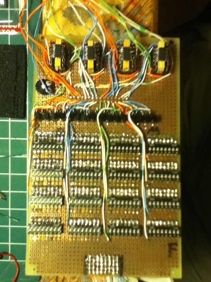
this is the top of the ROM board. on the right half of the picture you can see the 16 dip switches that make up the ROM, and on the right you can see the four LM339 comparators I had to use to repair the signals coming out of the multiplexer. in between are pnp transistors that are necessary to make the output of the LM339s useful as they are open collector circuits.
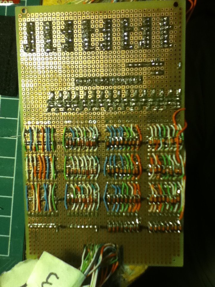
this is the bottom of the ROM board. I'm about 3/4 done soldering diodes onto the bottom of the board.
next steps:
the next section I will have to build is the control logic. this will take the individual machine code instructions and translate them into control bits (mostly flipping read write bits on registers). the most efficient way to build the control logic would be to build a 1:16 demultiplexer, but you saw how that turned out the first time around. I haven't been able to come up with a better way to turn binary numbers into individual pulses, but I don't think I can build such a large demultiplexer without needing to use comparators again, which I'd rather not do. anyway if you have any ideas about how to change binary numbers ito individual pulses or how to build comparators out of discrete components they would be welcome in the comments.
Discussions
Become a Hackaday.io Member
Create an account to leave a comment. Already have an account? Log In.