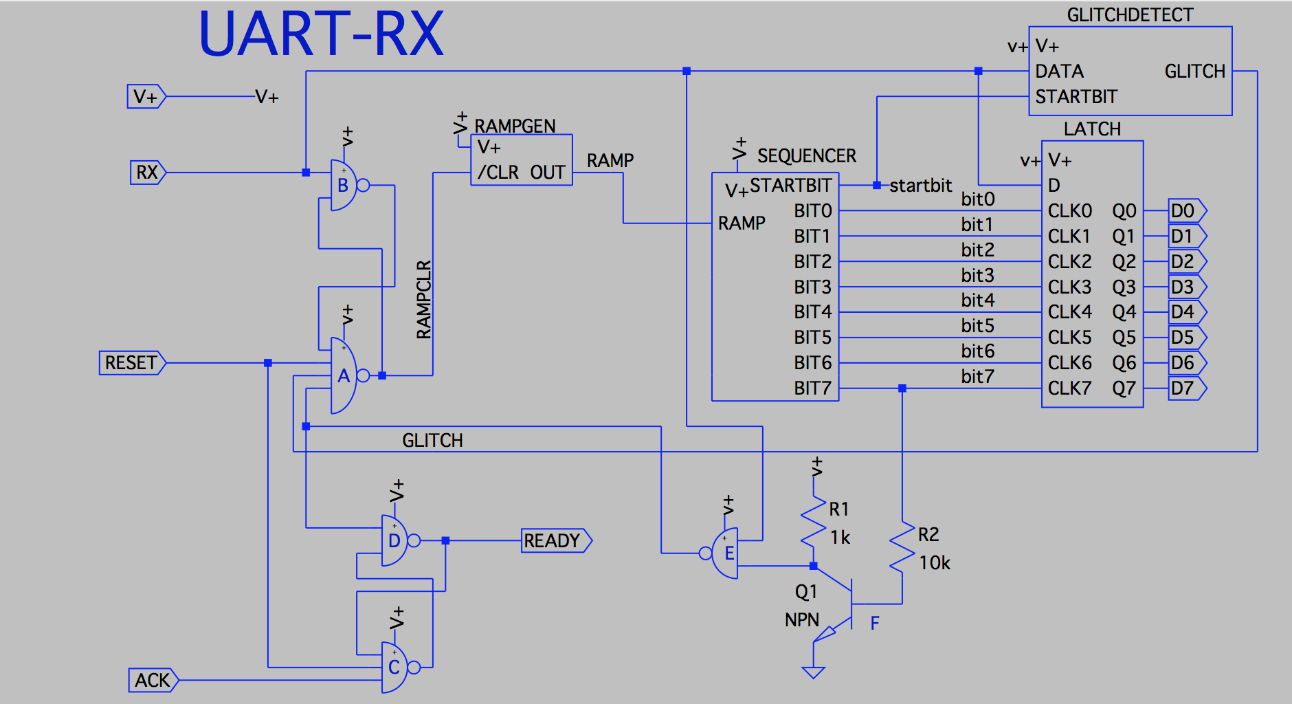
The board holds nine comparators, one ramp generator, one glitch detector and six NAND gates used connected as flip-flops to control the logic and sequencing.
The connector at left of the PCB
- RX-data (in)
- Master reset (in)
- Data Ready (out)
- Acknowledge/Data read (in)
- GND & V+
At the right site there's the connector to the D-latch board
- RX-data (out)
- 8 pcs of Latch clocks
- GND & V+
This is a modular view of the receiver (the LATCH-part is on a separate board)

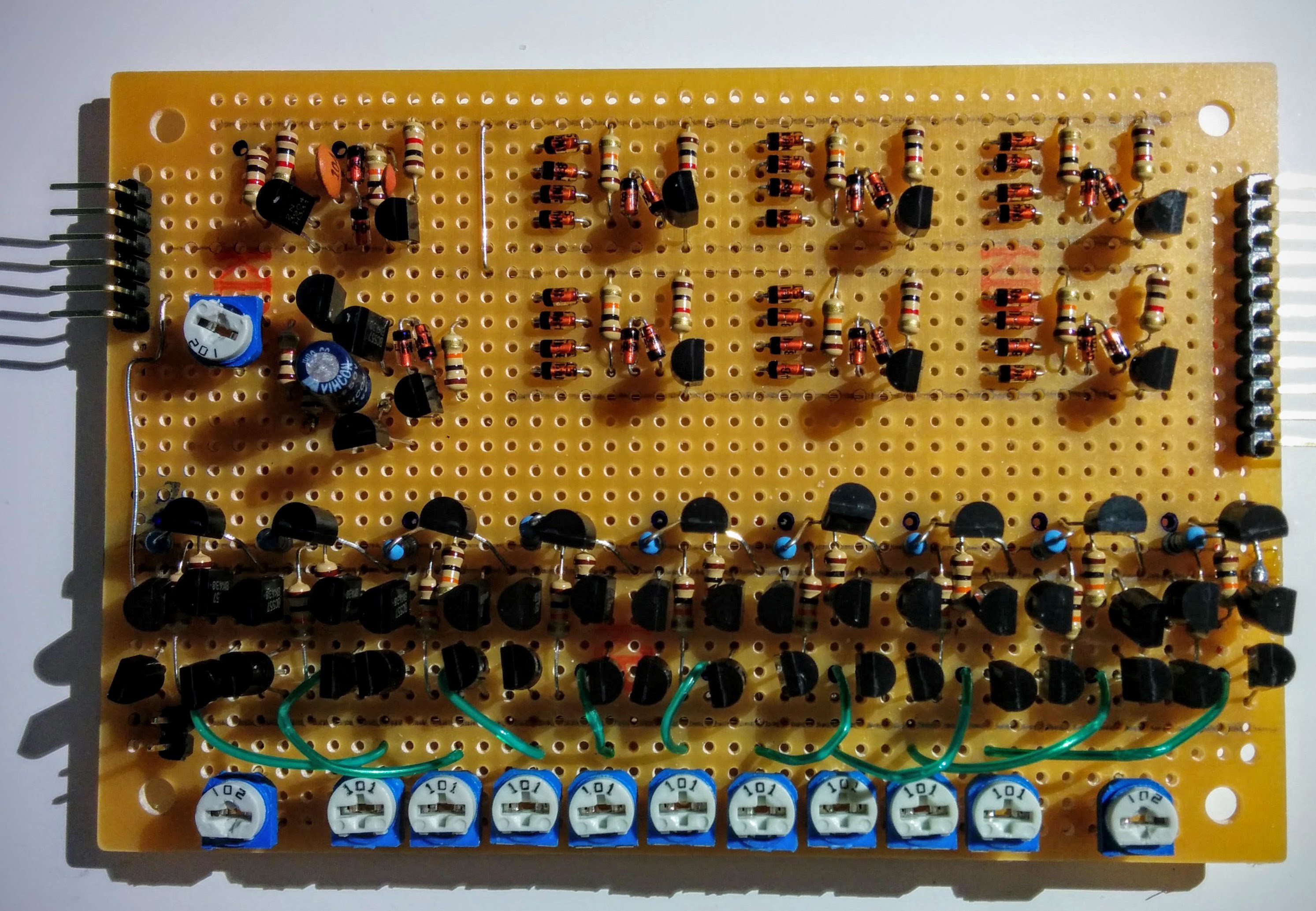
Before the logic wiring - beautiful (or at least ok)

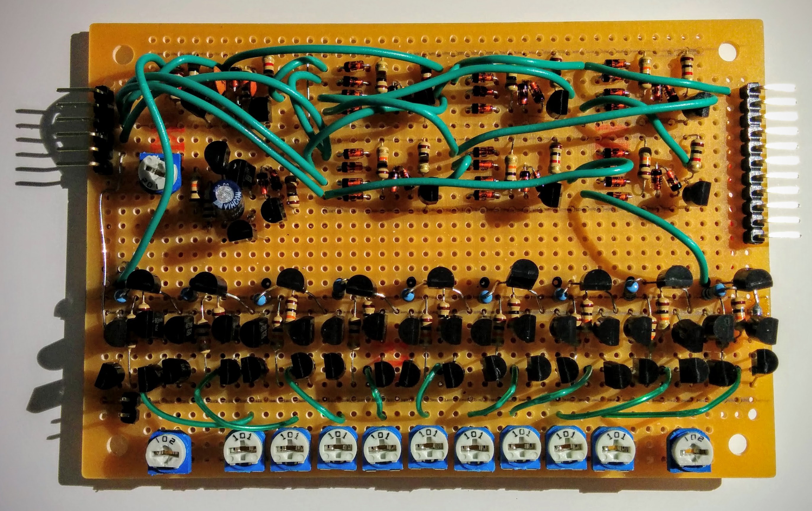
After the logic wiring - messy indeed

 matseng
Discussions
Become a Hackaday.io Member
Create an account to leave a comment. Already have an account? Log In.