 Yann Guidon / YGDES
With the diode ROM that "solves" the hexadecimal-to-7segments problem, it's now time to revise the design of the input FIFO.
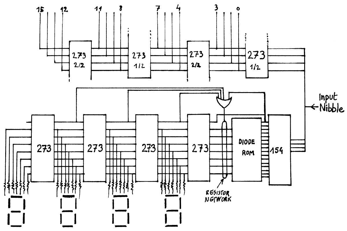
The 4-deep and 4-wide "shift register" is implemented by the same 74HC273 as before, this does not change (heh, it works, right ?). So 2× '273 are used for this function.
The changes are in the display logic. The TIL311 are nice for prototyping but they are expensive, not mass-produced anymore, consume a significant amount of power and are not thin or surface-mount devices. The display and decoding problems have been addressed separately, with ultra-thin 4014 LEDs and the diode ROM and it's time to put them all together.
Unfortunately, the diode ROM and the 4014 display are not practical for my prototyping method. I might assemble them separately and cut/saw the PCBs to make modules... I'll have to etch a proper PCB with the right patterns soon.
The input FIFO's display structure has changed because the TIL311 have individual hexadecimal decoders but the diode array can't be reasonably duplicated. The 4 hex digits will share one diode decoder, and a parallel shift register will propagate the value on the 7 segments, just like the nibble is propagated from LSB to MSB.
The '273 has 8 bits and one remains unused for the 7 segments. This extra bit indicates if the digit is '0' (when it's cleared, because it's the direct output of Y0 of the 74HC154) and this is propagated to some more logic to disable leading 0s. By chance, the '273 resets to all-0s so there is no logic inversion to do there.
Another nice trick: it's possible to play with the pull-up resistors of the diode array. Implicitly, it creates a "AND" gate when instead of pulling up, a logic gate decides to pull-down. All the segments will be off, this controls the leading zero digits. This goes a bit further than the schematic in "Redneck" disintegrated 7 segments decoder, where the extra input of the 273 was unused, but we could see the /Y0 output connected to the /CLR pin.

I have made a first hex display module with the utra-thin LEDs and the only thing I'm not sure, is the series resistor value. I'll see if/how I can make a module that contains all the circuits shown in the above diagram.
Update:
I modified the "leading 0" logic :
- the first '273's MSB is fed from the /Y0 directly, not from the OR, so when you input 0 after 3000h, the display will become blank
- the OR does not use the value of the last '273 because it will be discarded/pushed away by the next digit anyway.
Now, if a 0 is shifted in after 3000h was entered, the 3 remaining 000 MSB/digits should be cleared. That's some more logic to add to the CLR pin of the '273s... The output of the OR can be sent directly to the 4 CLR pins but this must also be combined with the "clear" external command. The external CLR can be combined by the OR and fed to the 3 MSB digits.
Why 3 digits ? When the input is blank, I'd like to have it display at least a 0 at the LSB so the reset local will not affect the LSB.
Damn I have to update the diagram again...
Discussions
Become a Hackaday.io Member
Create an account to leave a comment. Already have an account? Log In.