 Yann Guidon / YGDES
RAM is one big problem for "discrete projects". It must be fast, large and cost-effective. There are many types of discrete RAM but none that is based on discrete MOSFET (yet).
Integrated DRAM uses MOSFETs but they differ from the discrete form because of the intrinsic diode with the substrate : it takes two discrete MOSFET to make one normal MOSFET. This would not be cost-effective to use discrete MOSFET to implement classic DRAM circuits.
I found inspiration with the diode-capacitor cell described for the TIM computers :
I can't figure out what capacitance was used in the relay-based TIM8. However, with a MOSET-based circuit, the capacitance can be greatly reduced (to 100nF for example) because the required trigger energy is considerably lower. I even have a reel of dual Schottky diodes in SOT23. But I'm not sure about the leakage...
Now, a good MOSFET has a pretty low leakage. I have played around (on paper) and have come up with a topology that replaces the diode with a MOSFET. The gate capacitance is not used but the parasitic diode is !
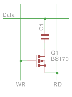
Each access cycle takes 2 steps:
- Read and empty the storage capacitor: drive RD high => This pushes the capacitor's lower electrode high, which is then read on the Data line. Probably a threshold current is required to read a "1".
- Write the value: drive the desired level on the Data line, drive RD to 0V and WR to 1 (let the current flow to RD so the lower electrode is 0V).
It's funny that the read phase works a bit like a charge pump...
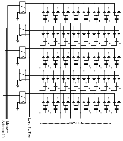
Data, RD and WR are totem-pole (complementary) drivers. I will have to try different circuits for the sense. The line and column select (demultiplexers) will need a lot of transistors too... But at least it's more compact than the only other MOSFET RAM that I know :-)
Now I wonder what should be the refresh frequency...
Any comment/remark/historical perspective ?
Discussions
Become a Hackaday.io Member
Create an account to leave a comment. Already have an account? Log In.
I know one MOSFET and one BJT is not just one MOSFET, but you might like to look at https://hackaday.io/project/19386-the-blinking-computer/log/158857-yet-another-memory-cell-2t which wires a BJT to the gate of the MOSFET. This way charge is stored on the MOSFET if the BJT is non conducting, but if it is conducting then it can be written. If there is charge on the MOSFET then it conducts, so it's easy to read.
Are you sure? yes | no
Why not a MOSFET per byte? Should work.
Are you sure? yes | no
Show us the whole circuit :-)
Are you sure? yes | no
Aha! Upon making it I found a problem : capacitor loops! Seems that you actually need diodes after all, and in the relay circuits too probably. So your diodes probably weren't in vain after all!
Are you sure? yes | no
who would have thought, right ? :-)
I'm glad we all learned a lesson here !
Are you sure? yes | no
Hi Yann,
I posted my addressable D-Latch (https://hackaday.io/project/13232-dtl-addressable-d-latch).
The design was stackable for bit depth (i.e. a byte), had a 3 bit address and open collector output (for the bus). Uses five transistor per bit excluding the address invertors.
Just an alternative to dynamic RAM.
AlanX
Are you sure? yes | no
Interesting... I'll keep that for my germanium experiments :-)
Are you sure? yes | no
Hi Yann,
So it works.
What would a 4x4 array look like with the decoding?
AlanX
Are you sure? yes | no
A 4×4 would be interesting to see.
I suspect capacitive coupling will start to appear between lines...
The decoders, for now, would be 74HC148 for sake of simplicity. That would make it 8×8 (8 bytes). But the question is still how to sense the spike/level. High impendance is a must to reduce currents.
Are you sure? yes | no
Wait, a single '148 would work with 4 pairs of lines, since the WR and RD signals are never ON at the same time.
Are you sure? yes | no
Basically the sense amp is a pair of inverters with positive feedback (a latch) that you intentionally shorted together initially. While it is sitting on the fence trying to figure out which way to go, you connect up the cap and because of the charge in the cap would push the logic to go '0' or '1'. Since the cap is connected, the act of reading also refreshes the capacitor with the full voltage. I would assume that writing to the DRAM would involve flipping the bits on the sense amp and then read the cell.
The DRAM refresh time is determined by how sensitive the sense amp is, amount of leakages and the capacitance. The capacitance (and parasitics) dictates on how fast the device can be read/write.
http://www.google.com.na/patents/US20130083590
"Sense amplifier using reference signal through standard mos and dram capacitor"
Are you sure? yes | no
"That escalated quickly" :-D
Are you sure? yes | no
I would agree with Lee.
Many "simple" ideas become more complex as you build them up.
I would design a demo memory unit before locking in the concept for a bigger project.
I did an addressable D-Latch in DTL on strip-board. Simple and effective but more components. With a PCB it is just more components and soldering. For a simple CPU it is doable for small memory arrays. If you like I can post the basic design.
Regards AlanX
Are you sure? yes | no
Wiring something up right now :-D
Are you sure? yes | no
Initial basic expectations are met, so far... The charge pump seems to work.
Detection of the capacitor charge is less trivial however. My scope probes discharge the storage cap...
Are you sure? yes | no
Well if I'm quick enough :
* when reading a cleared cap, I get a +3V spike on the Data line
* when the cap is charged, I get a +6V spike.
I'd need a sort of voltage translator to detect a voltage above 4.5V...
Are you sure? yes | no
You can offset a N-MOSFET such that its VTH is set at 4.5V.
Ideally if you use one with VTH = 1V or so to get a tighter tolerance. Now you can connect the drain to Vcc=3V3. Add a pull down to the source which is the output and that's your sensor.
Are you sure? yes | no
@K.C. Lee yeah, I was trying to figure out something like that. Now it makes sense (no pun intended) and should work very well.
Further select is achieved by other N-FET that connect the selected pull-down to 0V so different lines can be shared for one data output... LOVELY.
Are you sure? yes | no
The size of the cap is dependent on the overall parasitics (MOSFET have all kinds of capacitances). The charge from the cap has to redistribute between the parasitics capacitance results in a lower voltage. Too high, then you are wasting power when you overwrite a bit to its complement and slowing the access time.
At a system level, you'll need logic to generate the timing sequence to read DRAM and refresh them. That's adding complexity and timing constraints.
Are you sure? yes | no
@K.C. Lee I just tried what you described and ...
It doesn't seem to work :-(
I increased the capacity from 100nF to 470u to reduce the scope's influence. I'm working at 3V. I get a peak at 5Vsomething, due to the drop in the MOSFET's diode.
So far the detection side escapes me but that's something cool to sleep on.
Read you tomorrow :-)
Are you sure? yes | no
Remember that VTH has to be 1V (max) for this to work. 1V (max) + 3.3V = 4.3V (max)
If you use 2N7002, your threshold can be as high as 3.3V + 2.5V(max) = 5.8V!
2N7000 has VTH = 3V (max).
The large (min) & (max) range of 1V to 2.5V makes it hard to detect the voltage with older MOSFET.
Are you sure? yes | no
No it's not about Vth.
anyway Vth is measured from source to gate. The gate is "floating" when no read is selected so I get AC hum/buzz. Then when doing the cycles (by hand) I get totally inconsistent results.
When the drain is set to +3V, what actually matters is the source voltage... which will float too depending on the gate voltage, which also floats...
Are you sure? yes | no
MOSFET doesn't care too much about flipping source and drain as they are symmetrical. The only reason for reversing the connection is because of the body diode. This is how one would use a N-MOSFET for the high side of a H bridge.
The sense line will be floating. The trick is to precharge the (capacitance) of the line first if you want a really high impedance. :P Dynamic logic uses tricks like this. Or have a resistor to pull it to something.
Are you sure? yes | no
precharge... hmm...
My current test circuit is getting crowded and I might have to solder it instead.
Before you sent your method, I was thinking of charge-pump-like system with a "precharge" of a capacitor with a diode from +3V. Then the read pulse raises the source of the sense FET. If the data pulse is higher than threshold, it will empty the capacitor. However, timing issues and race conditions will become hard to solve...
Are you sure? yes | no
For low density, it isn't that much more effort to build 4T SRAM using a couple of dual MOSFET and 1/2 resistor network. It solves the issue of having to refresh the DRAM, building sense amp and deal with timings.
Are you sure? yes | no
Hi Yann,
Okay got that missed the builtin (zener/protection) diode.
The high transistor count is a fact of life (my 8 bit CPU is equivalent to about 800 transistors (yes I have counted!) excluding RAM/ROM). There is no escaping it. That is why we need to explore high level architecture first.
Well completing your bit RAM is then no big headache, just need row and column address decoders, read/write logic and a sense amp (a high impedance transistor voltage follower should work here). Just copy a 74LS138 gate design for the decoders. I think you will need two decodes for the rows and two for the columns in order to implement the read/write logic (otherwise you will need three gates per row and column line for the read/write logic).
My personal approach is diode transistor logic (DTL) but there are other systems. As your using 2N7000s I would look at gate logic built on that. Due to the gate capacitance they may be slower than DTL but I have not researched it.
Regards AlanX
Are you sure? yes | no
It's not a Zener nor a protection diode but intrinsic from the connexion of P and N doped regions, which creates a diode...
Decoders will take a lot of effort, I know :-D There will be quite some capacitive effects too...
Gate capacitance is not really a problem with complementary MOSFETs. Power is good too because there is current only during transitions.
Are you sure? yes | no
Hi Yann,
I have seen TIM-8 before and yes the design is pretty neat.
My initial thoughts were to replace the relays with CMOS analog multiplexers.
A three components per cell and simple read/write.
Just pushing the read high and keeping the write low to read the capacitor voltage does not work as the mosfet is hard off (unless you are relying on "varicap" properties of the drain/source or diode parasitic capacitance or something like that)? Unless I have missed something fundamental here.
Refresh rate will depend on the internal/leakage resistance of the capacitor.
Tantalum would probably work well but I would be driven by cost here.
The answer is to test your circuit and report your results.
Use an Ardunio for the read/write signals (digital) and see if you can analog read the cell. Failing that more research is required! - Has someone else done this?
My approach would be a little different.
For the CPU ROM I would go with discrete PLA as the gate count is less than 2 per byte. The ROM is still programmable (using DIP switches) but "not as we know it".
For the RAM I would make the following observation.
These are "demo" CPUs and the demo programs do not need much RAM.
Eight to sixteen bytes should be enough. The standard D-Latch register memory will work here.
At the end of the day your project will sit on your shelf (hopefully power up) and demonstrate you have mastered the CPU. Unlike "MyCPU" (http://www.mycpu.eu/) we are not really going to build something that will replace our laptops.
Something else to consider very early in your project is the interface. It is a project killer if you don't. You will note that I use a front panel. Stepping up from that is really hard work (CHIP-8 is an option).
Anyway I have rambled on a bit, regards AlanX
Are you sure? yes | no
Hi ! Lots of interesting stuff to ramble about, thanks ;-)
> Just pushing the read high and keeping the write low to read the
> capacitor voltage does not work as the mosfet is hard off (unless you
> are relying on "varicap" properties of the drain/source or
> diode parasitic capacitance or something like that)? Unless I have
> missed something fundamental here.
You are missing the parasitic diode that overrides the MOSFET when it is hard off. Try yourself with a 2N7000 or somesuch ;-)
Refresh rate : I'd go with 100nF in 1206 for ease of soldering, and "to show the kids". I might have a reel of 330nF/50V too but too much capacitance will increase the working energy and slow down the whole device. Yes, working frequency is good to keep in mind ;-)
This would not be intended for program storage, at first I think. I am "shopping around" for a 8-bits CPU with 256 bytes of RAM... Program would be somewhere else, maybe a diode/switches array ?
A D-latch requires at the very least 2 transistors. CMOS makes it 4, then you need addressing and shorting transistors... such a high count is OK for the registers but DATA RAM ?...
And no, it's not to replace my laptop (I have F-CPU for this :-P) but I want to involve kids so it must be simple, cheap and reliable.
And for the interface, I'm working on this ( #DYPLED etc.) with experience from #Discrete YASEP
regards :-)
Are you sure? yes | no