 Patrick Van Oosterwijck
Initial test results are in!
I used my electronic load to see if the wESP32 prototypes would achieve my target of 12.95W output power to meet the 802.3at Type 1 PoE specification. Here's my setup:
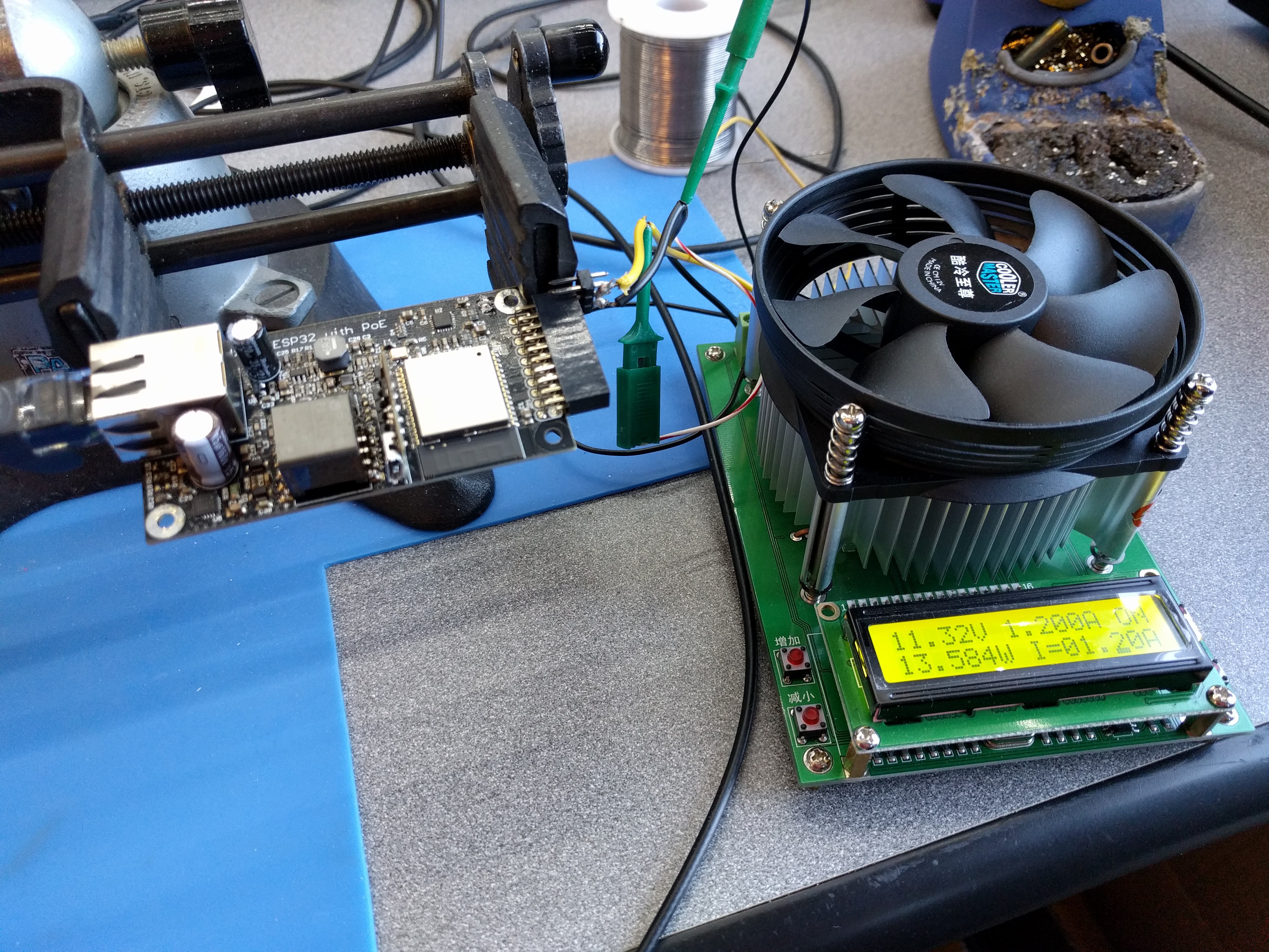
Yes, you are seeing that correctly on the display of the electronic load: 13.5W! What's more, I kept it running like this for a couple of hours and it was stable! No over current or thermal shutdown. And this is without any heat sink attached to the mounting hole! I never expected I would get full target power without extra heat sinking.
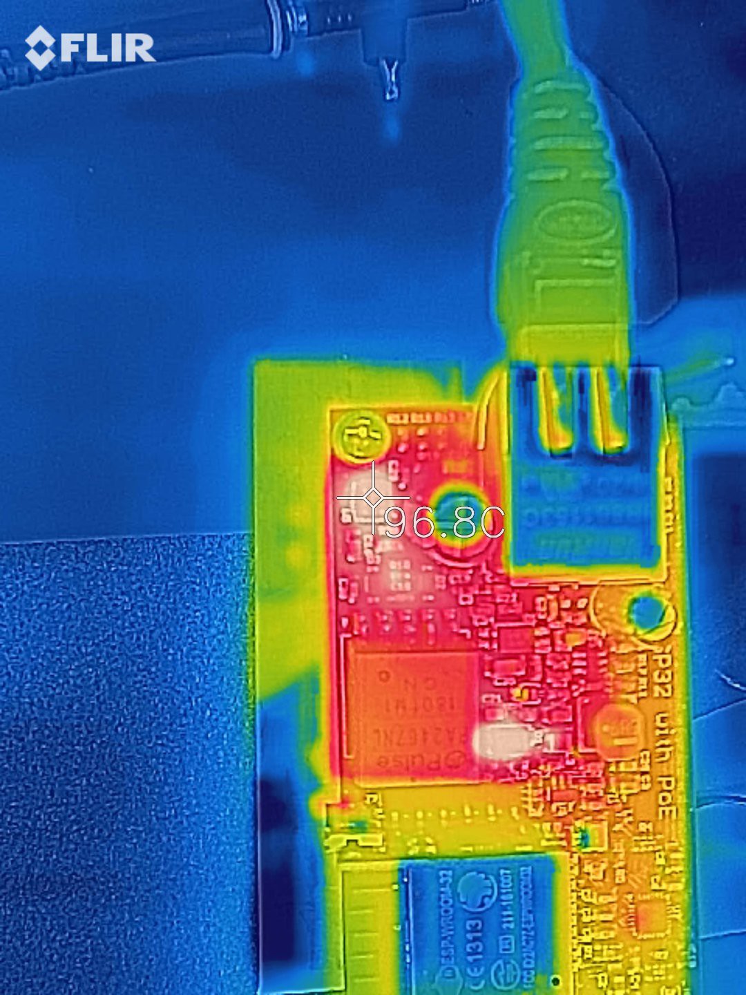
The hot spots are as expected the Si3404A PoE power converter chip and the secondary side Schottky rectifying diode. The diode is hot, but it's within acceptable limits:
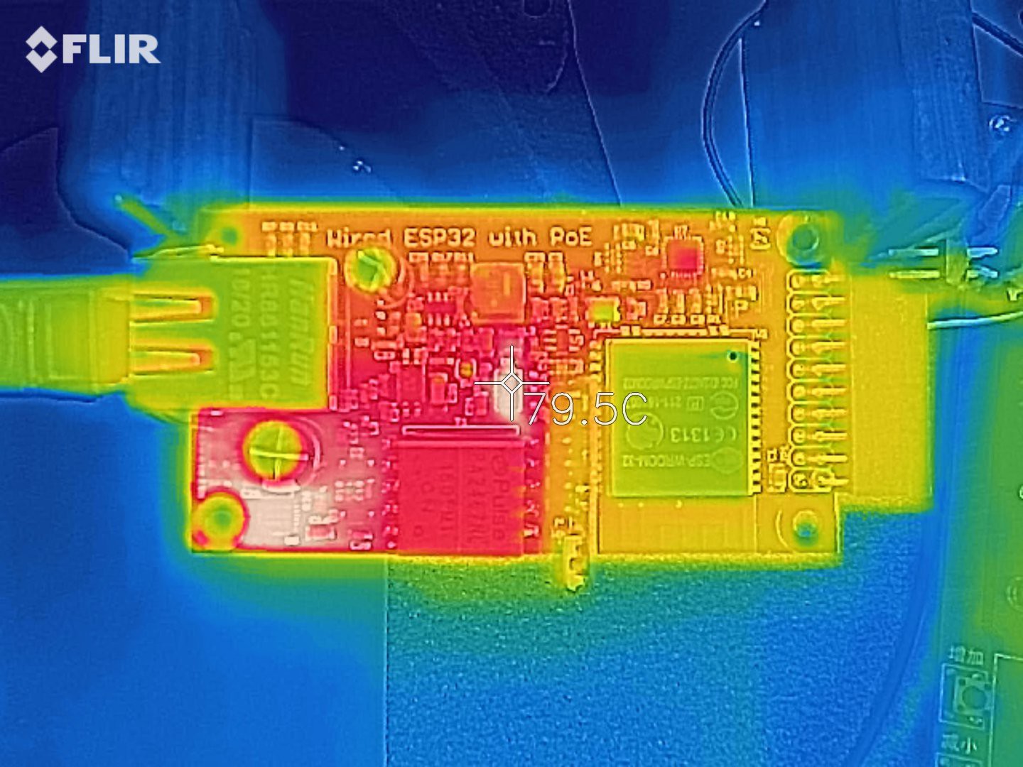
The power chip is getting much hotter, not enough to trigger over temperature protection apparently, but too hot to run like this for a long time:

Although it works, I would not recommend running at full power without any heat sinking. So how much difference does connecting a heat sink to the mounting hole actually make? Let's find out:
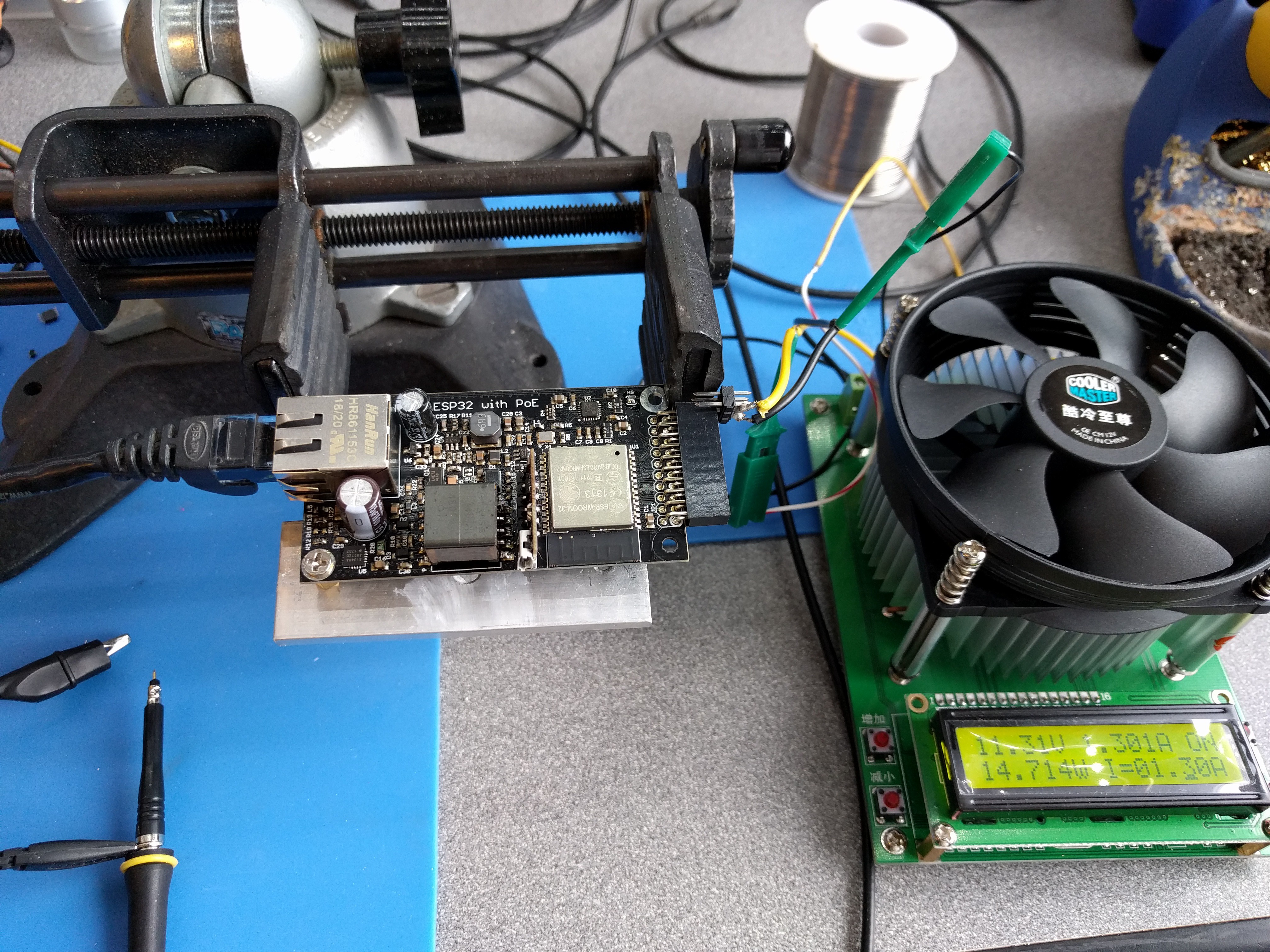
It may be noted that I'm not trying very hard here to provide an optimal heat sink. I'm just using a flat piece of aluminum with a stand-off screwed into it, screwed to the mounting hole. No thermal grease is used.
As you can see, I decided to really push it and bumped power up to 14.7W. This was stable with the extra heat sinking. Of course, the diode got a little hotter now:
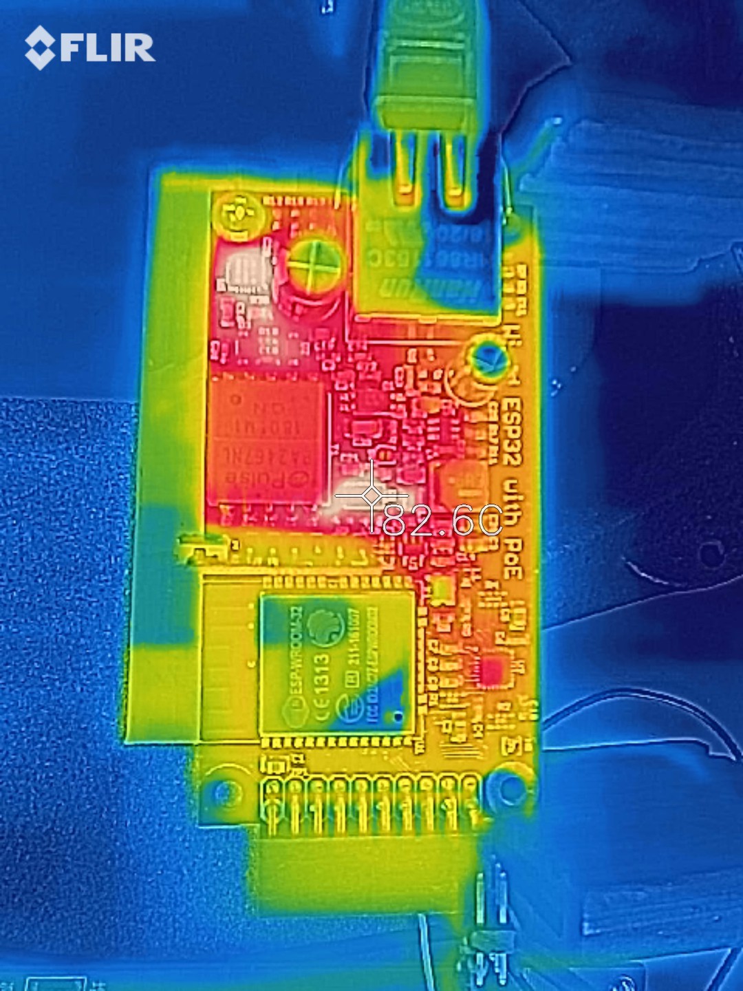
Still perfectly acceptable. The power chip on the other hand is cooler now, because the heat sink is doing its job pulling heat away from the chip:
I decided that to compare apples to apples, I better reduce the output load to the same 13.5W as before so I could see how much difference in temperature the heat sink actually makes:
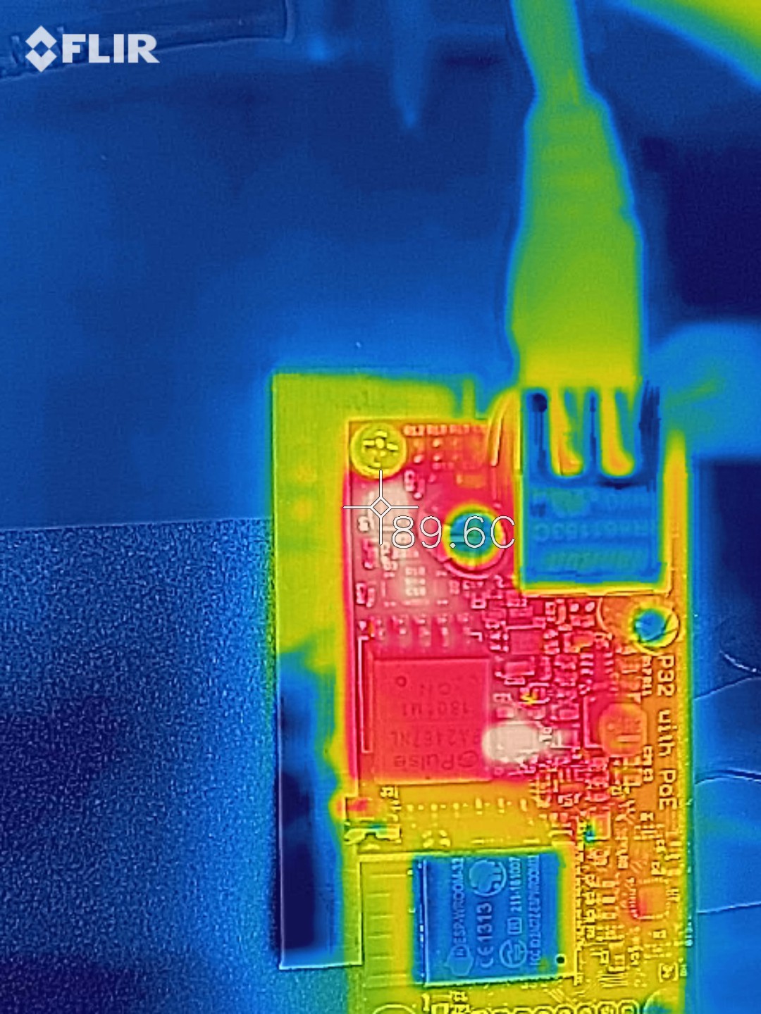
That's 25°C cooler, at an acceptable temperature while running at a load that's higher than demanded by the spec. I call that good enough. :)
An interesting detail in the latter thermal images: the resolution is good enough to see a couple more small hot spots: one by current sense resistor R20 and one by resistor R10 of the RCD clamp. Both are normal and expected: the current sense resistor senses the current through the primary winding and will dissipate around 0.1W under high load, while the RCD clamp is there to dissipate energy from self-inductance of the primary flyback winding, to prevent this energy from resonating and producing large (noisy and potentially damaging) voltage spikes.
It should be noted that in all these tests the actual load is a little higher than what I see on the electronic load display because the 3.3V buck converter, ESP32 and Ethernet Phy consume some power as well. But I decided to ignore it for these tests since it's less than 0.5W or so.
So how does the flyback converter's output power look? How much noise is on it under various loads? I had planned to show some scope traces, but I decided against it because they were very boring: just a flat line. :) That's excellent! Even under the highest load, the V+ power bus looks very clean. I haven't had this design tested for EMI but if/when I do, it looks like it may be fine.
Very happy with these results. Next, I need to check what happens when 5V output is selected, and try to figure out what's wrong with the two prototypes that aren't fully functional, plus build some more prototypes for the people who are waiting to buy them for their own testing.
Discussions
Become a Hackaday.io Member
Create an account to leave a comment. Already have an account? Log In.
Nice!
Are you sure? yes | no