 Pinomelean
I had to redesign the circuit i used in v1.0 to fix the problems it created, and with such a simple circuit to begin with, that meant starting from scratch again.
(V1.0 circuit diagram for reference)
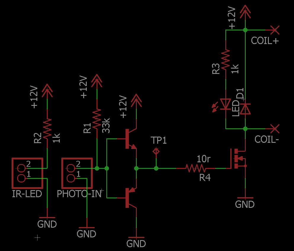
The first thing that i noticed in v1.0 is how slow was the voltage ramp at the MOSFET gates. I traced the problem back to the photodiode itself. As you can see in the diagram above, the signal at the the photodiode output is the same as the VGS applied to the mosfet (the BJT pair just increase the current availible to the gate). As i've mentioned before, this slow ramp at the MOSFET gate is a likely cause of the many explosions they produced. In a high current application such as this, the MOSFETs should only work as switches, in the saturation region, this meant i had to reduce drastically the ammount of time they spent switching ON, in the linear region.
As a side note i should point out that the MOSFETs switched OFF orders of magnitude faster than ON, and the schottky diode absorbed the induction spike just fine, leaving no trace of overshoot at all.
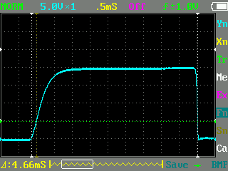
This is the voltage at the MOSFET gate in the first stage (the one with longer ON time and the most likely to explode). It's also taken when i was using 24v to drive the gates, which was changed to 12v shortly after.
You can see that the MOSFET was working in its linear region for almost 2ms. This is what i needed to change.
Other aspect i wanted to change about the rifle as a whole is the sequence in which the coils activate. In v1.0 only one coil was ON at any time, which was the simple way of doing things.
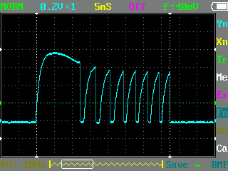
This is the voltage measured accross a 7mOhm resistor in series with the whole gun.
We can see that its current draw peaked at ~110A with the first coil, but the other 7 coils didn't reach their steady-state; they never got to completely build up their magnetic field, which happens when they draw the full current as in a DC situation.
This means that most coils never turn fully ON, and never get to apply the maximum force they could on the projectile.
I decided to improve the v2.0 design by switching ON the coils several stages ahead of the projectile, so when the bullet is about to reach that coil, it has had time to fully build up a field and impart the most ammount of force it can. The stages still have to turn OFF as the projectile is in the middle of their coil, so as to not slow it down at all.
This meant that i had to design a circuit that would switch ON the coil when receiving an external signal (from a previous stage) and still switch OFF by itself when it detects the projectile.
The following diagram is what i came up with:
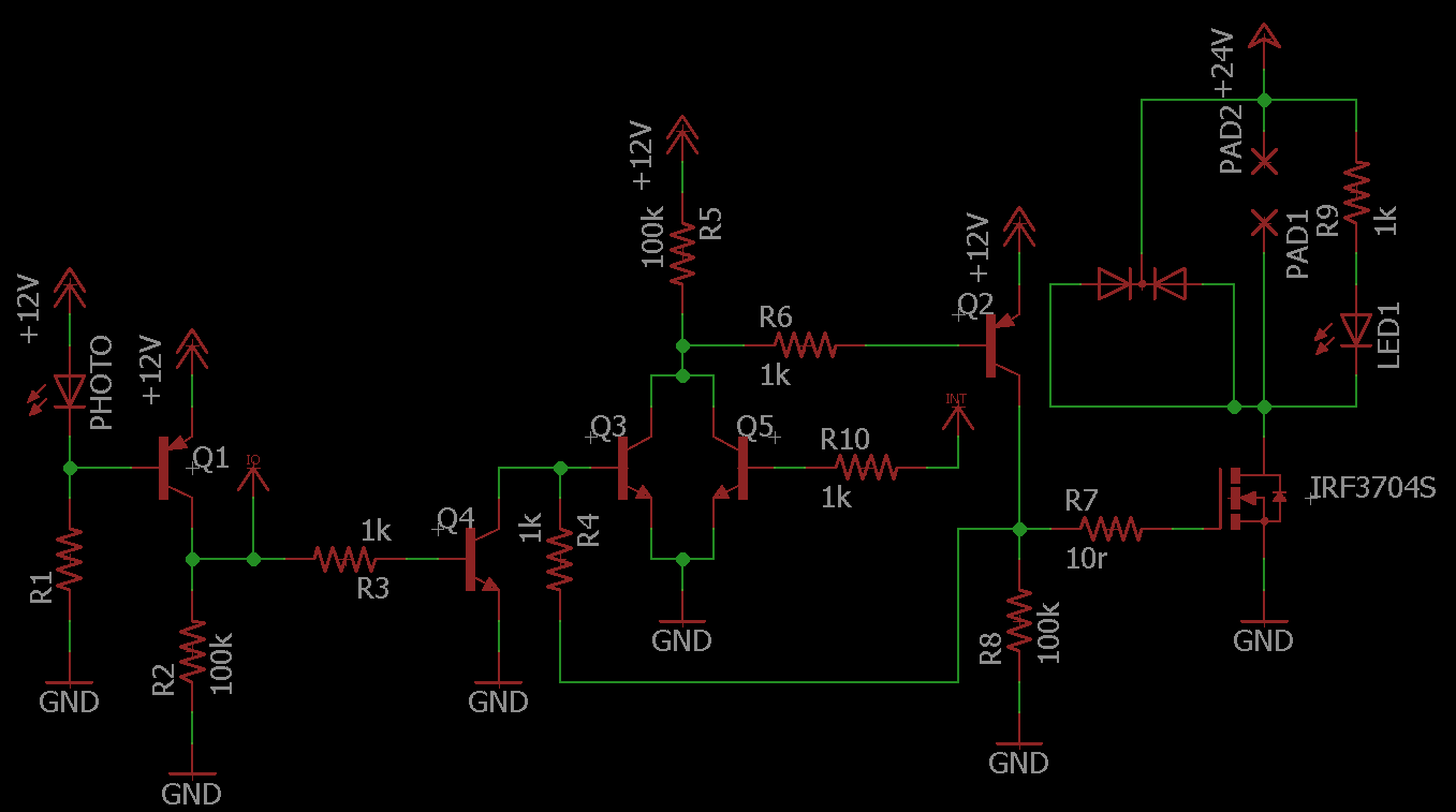
The signal that switches ON the coil enters each stage at the supply syimbol with INT on it. A logic 1 (+12v) on this point will turn ON Q5, which will in turn pull down the base of Q2. Q2 pulls high the MOSFET gate and also the base of Q3, which closes this positive feedback loop that keeps the MOSFET ON even when the signal coming from a previous stage (the +12v at INT) drops low again.
When the projectile reaches the end of the coil (it will be in the middle of the coil if they have the same lenght) the IR bridge will be broken and the voltage at the base of Q1 will drop.
With this circuit it doesn't matter if it takes 2ms for the voltage accross the photodiode to reach ~10v, which was the point at which the MOSFET would be fully ON in v1.0.
Here, as soon as the photodiode is a bit shaded, the voltage at the base of Q1 will drop below VCC-0.7v (switching Q1 ON) and it will start conducting current through R2. The supply symbol with IO on it is at the voltage accross R2, and is the signal sent to a stage ahead of this one in order to turn that one ON.
This signal also turns OFF the coil of its own stage by pulling up the base of Q4, which in turn pulls down the gate of the MOSFET.
The two diodes in parallel with the coil (PAD1 & PAD2) are two schottky diodes is a single package, the energy stored in the coil when the MOSFET switches OFF is dissipated in these diodes, preventing the formation of a HV spike that could destroy the MOSFET.
The LED just signals when the coil is ON.
With this circuit, it takes mere microseconds (μs) instead of milliseconds (ms) for the ON signal to reach 12v. Switching ON the MOSFET this much faster will avoid the power dissipation that was probably the cause of many unwanted fireworks with v1.0.
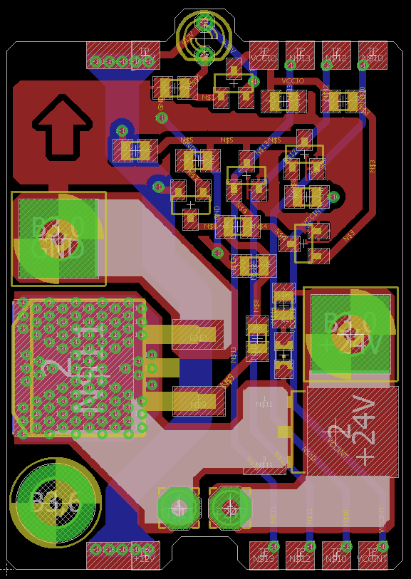
This is the PCB i designed:
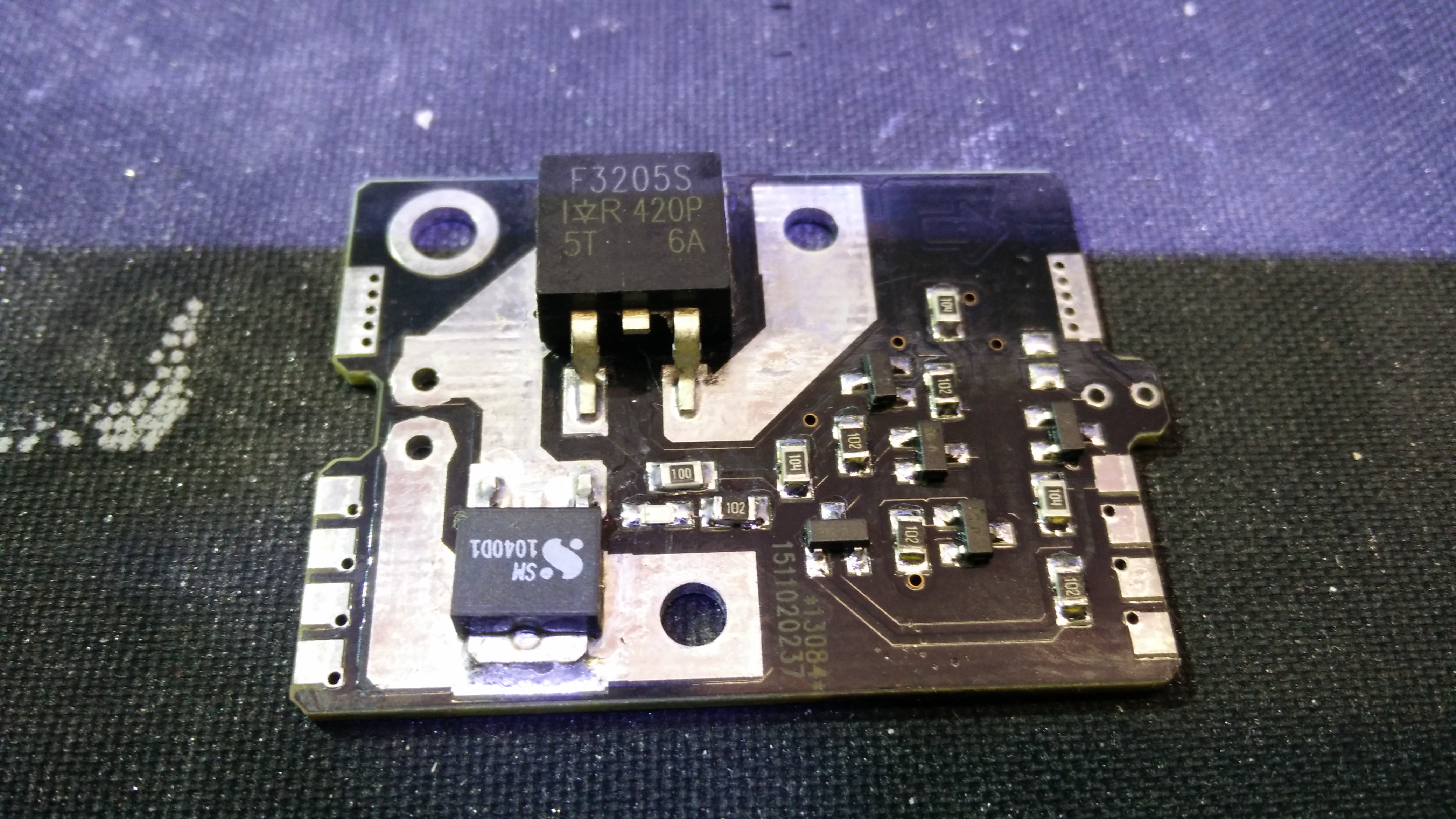
A populated v2.0 PCB:
V1.0 PCB for comparison:
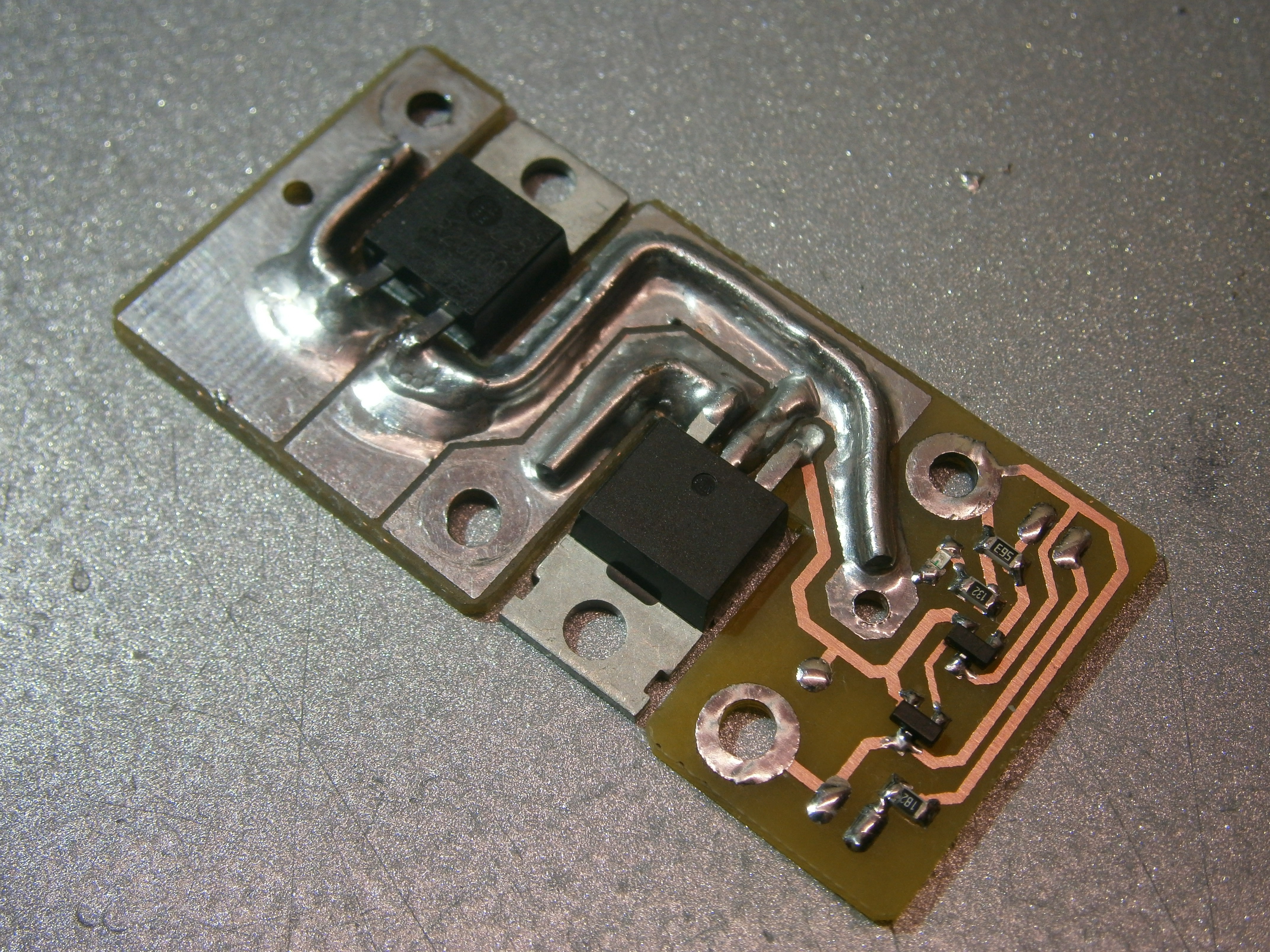
It is shorter than those used in v1.0, wich were 6cm long. This ones are also as long as the distance between coils (this time will be 4cm). I got the size down by using all SMD components, except the IR photodiode. The biggest component is the MOSFET, followed by the dual schottky diode.
The PCBs will be connected to the power rails by M3 screws like in v1.0, and the MOSFET driver circuit will be powered by a 12v line wich runs through the bottom layer and will connect between boards with a solder bridge using the exposed pads in the top and bottom left of each board. The pads on the right will carry the projectile detection signal up to four boards ahead, wich will power up the target coil.
Discussions
Become a Hackaday.io Member
Create an account to leave a comment. Already have an account? Log In.